Operational amplifier and analog-digital converter with inductor and double power supplies
An operational amplifier, dual power supply technology, used in amplifiers with semiconductor devices/discharge tubes, DC-coupled DC amplifiers, amplifiers, etc., can solve problems such as limiting the overall performance of ADCs, improve phase margin, and speed up the establishment of Time and performance improvements
- Summary
- Abstract
- Description
- Claims
- Application Information
AI Technical Summary
Problems solved by technology
Method used
Image
Examples
Embodiment 1
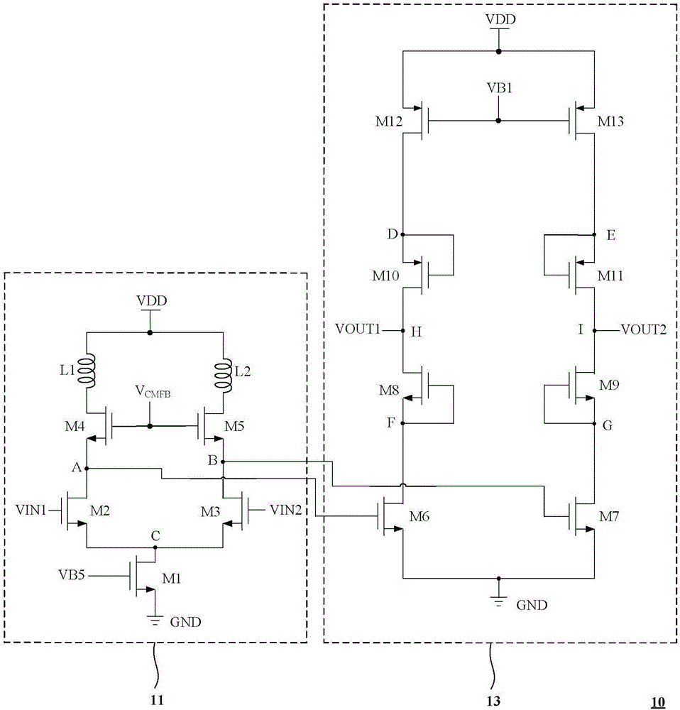
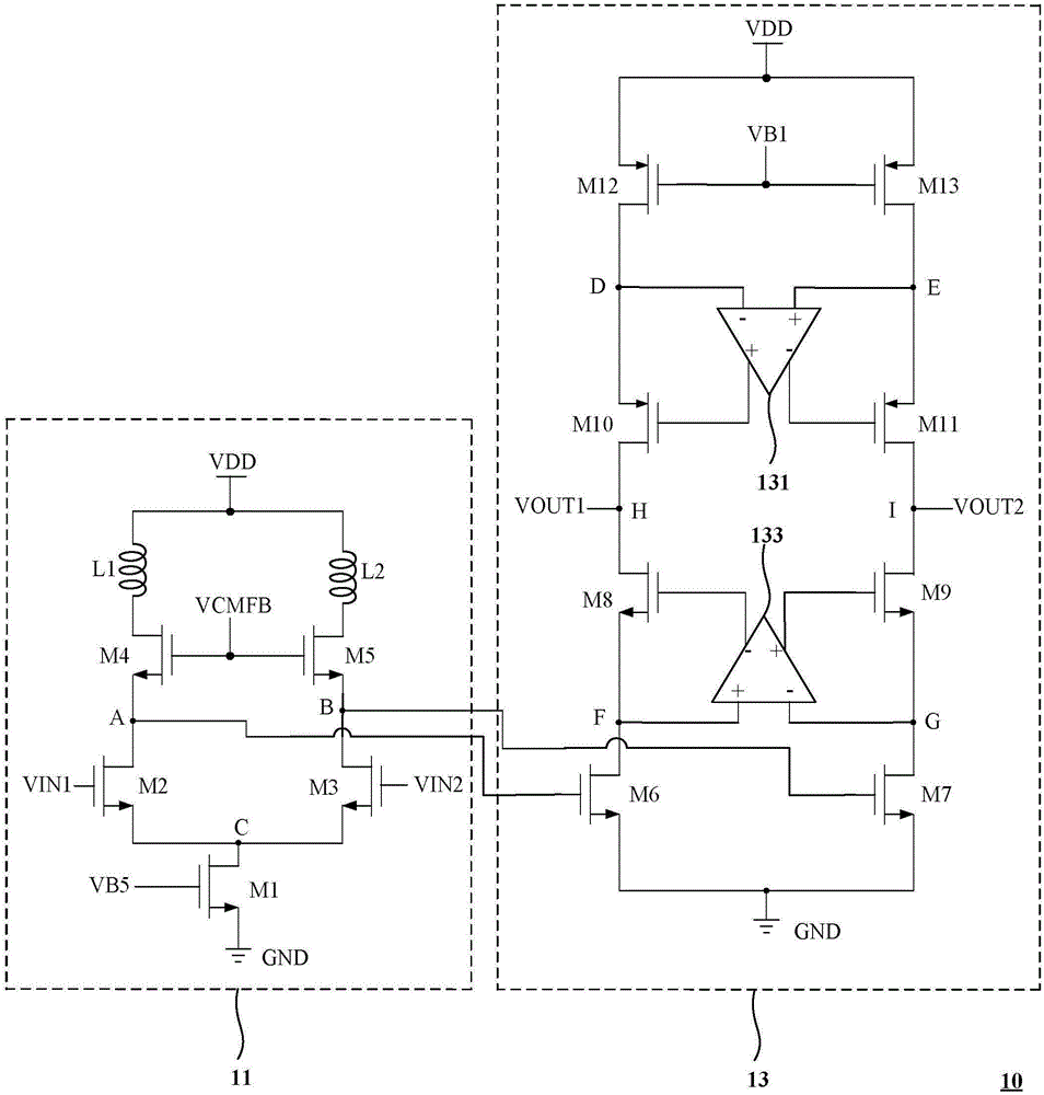
[0040] See figure 1 , figure 1 It is a schematic diagram of a circuit structure of an operational amplifier powered by dual power supplies with inductance provided by an embodiment of the present invention. The operational amplifier 10 powered by inductive dual power supplies includes a preamplifier 11 and a main amplifier stage circuit 13; the preamplifier 11 includes a first switch M1, a second switch M2, a third switch M3, a fourth switch M4, and a fifth switch M5, the first inductance L1 and the second inductance L2; the main amplifier stage circuit 13 includes the sixth switch M6, the seventh switch M7, the eighth switch M8, the ninth switch M9, the tenth switch M10, the eleventh switch M11, the The twelfth switch M12 and the thirteenth switch M13.
[0041] Specifically, the first inductor L1, the fourth switch M4, the second switch M2, and the first switch M1 are sequentially connected in series between the voltage source VDD and the ground terminal GND; the second ind...
Embodiment 2
[0050] In this embodiment, on the basis of the above-mentioned embodiments, the working principle and connection relationship thereof will be further described with emphasis.
[0051] see again figure 1 , the operational amplifier 10 includes a preamplifier 11, which is composed of M1-M5, L1, and L2. It adopts a simple active load common-source amplifier, uses M2, M3 as input tubes, and uses NMOS tubes M4, M5 as loads. Two inductors L1, L2 are connected in series above M4, M5.
[0052]The preamplifier 11 is powered by a power supply voltage VDD of 1.2V, which can reduce circuit power consumption while ensuring that all MOS transistors work in a safe area. The input tubes M2 and M3 adopt the minimum channel length to make the circuit faster. Because the preamplifier 11 only provides low gain and introduces the secondary point of the overall operational amplifier 10 at its output end, the load transistors M4 and M5 also use the minimum channel length to reduce parasitic capaci...
PUM
 Abstract
Description
Claims
Application Information
 - R&D Engineer
- R&D Manager
- IP Professional
- Industry Leading Data Capabilities
- Powerful AI technology
- Patent DNA Extraction
Browse by: Latest US Patents, China's latest patents, Technical Efficacy Thesaurus, Application Domain, Technology Topic, Popular Technical Reports.
© 2024 PatSnap. All rights reserved.Legal|Privacy policy|Modern Slavery Act Transparency Statement|Sitemap|About US| Contact US: help@patsnap.com


