Fingerprint image capturing device and fingerprint image capturing module thereof
A fingerprint image and capture module technology, which is applied in the acquisition/organization of fingerprints/palmprints, image communication, print image capture, etc.
- Summary
- Abstract
- Description
- Claims
- Application Information
AI Technical Summary
Problems solved by technology
Method used
Image
Examples
no. 1 example 〕
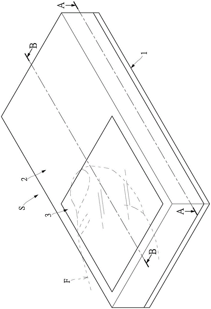
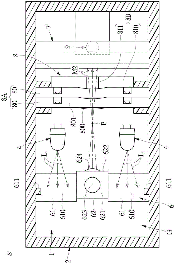
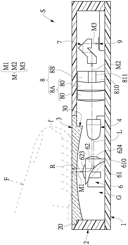
[0049] see Figure 1 to Figure 3 shown, where figure 2 for figure 1 A schematic cross-sectional view of the A-A secant line, image 3 for figure 1 Schematic cross-sectional view of the B-B section line. As can be seen from the above figures, the first embodiment of the present invention provides a fingerprint image capture device S, which includes: a circuit substrate 1, an outer shell 2, a light-transmitting element 3 and a fingerprint image capture module G, wherein The fingerprint image capture module G is arranged in the outer casing 2, and the fingerprint image capture module G includes at least one light-emitting element 4 (the accompanying drawings of the present invention use at least two light-emitting elements 4 as an example for illustration, but this is not the case. limited), a first optical element 6 , a second optical element 7 , a lens assembly 8 and a fingerprint image sensing element 9 .
[0050] First, cooperate figure 1 and image 3As shown, the out...
no. 2 example
[0059] see Figure 4 to Figure 5 As shown, the second embodiment of the present invention provides a fingerprint image capture module G, which includes: at least one light-emitting element 4 (the accompanying drawings of the present invention use at least two light-emitting elements 4 as examples for illustration, but do not use This is limited), a first optical element 6 , a second optical element 7 , a lens assembly 8 and a fingerprint image sensing element 9 .
[0060] Furthermore, the first optical element 6 is disposed on one side of at least one light-emitting element 4 and a first predetermined distance away from at least one light-emitting element 4, and the first optical element 6 has two reflective structures 61 and a connection The light guiding structure 62 between the two light reflecting structures 61 . Each reflective structure 61 has a reflective curved surface 610, and the light guide structure 62 has a first platform 621 facing the light-transmitting element...
PUM
 Abstract
Description
Claims
Application Information
 - Generate Ideas
- Intellectual Property
- Life Sciences
- Materials
- Tech Scout
- Unparalleled Data Quality
- Higher Quality Content
- 60% Fewer Hallucinations
Browse by: Latest US Patents, China's latest patents, Technical Efficacy Thesaurus, Application Domain, Technology Topic, Popular Technical Reports.
© 2025 PatSnap. All rights reserved.Legal|Privacy policy|Modern Slavery Act Transparency Statement|Sitemap|About US| Contact US: help@patsnap.com


