Anti-electromagnetic interference resistive memory and preparation method thereof

An anti-electromagnetic interference and resistive memory technology, applied in the field of microelectronics, can solve the problems of polluting the surrounding environment, accelerating waste of electronic devices, and detrimental to human health, and achieves the effects of simple process, efficient electromagnetic shielding, and excellent electrical conductivity.

Active Publication Date: 2019-09-24
GRIMAT ENG INST CO LTD
View PDF4 Cites 0 Cited by
  • Summary
  • Abstract
  • Description
  • Claims
  • Application Information

AI Technical Summary

Problems solved by technology

In the process of transmitting signals and utilizing electric energy, these electronic devices will cause electromagnetic interference to electronic components, affect the performance and service life of the equipment, accelerate the generation of waste electronic devices, pollute the surrounding environment, and are not conducive to human health.

Method used


Image

  • Anti-electromagnetic interference resistive memory and preparation method thereof
  • Anti-electromagnetic interference resistive memory and preparation method thereof
  • Anti-electromagnetic interference resistive memory and preparation method thereof

Examples


Embodiment 1

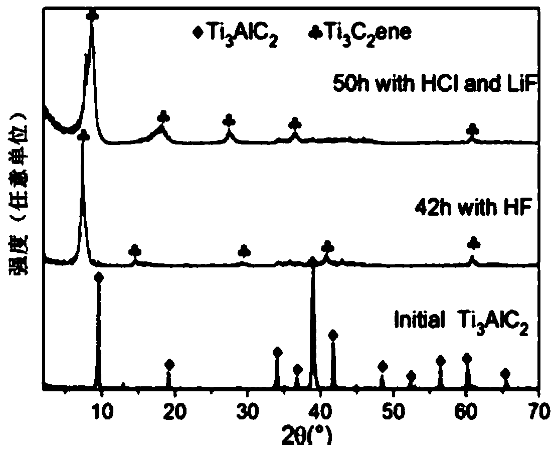
[0025] Electromagnetic shielding electrode material Ti 3 C 2 The preparation method of ene film specifically comprises the following steps:

[0026] Step 1: 3 g of Ti with a particle size of 45 μm 3 AlC 2 The powder is placed in a tetrafluoroethylene beaker filled with 35ml mass fraction of 40% HF;

[0027] Step 2: heating at 40°C for 42 hours, then naturally cooling to room temperature;

[0028] Step 3: Prepare the obtained black liquid, and wash it several times with deionized water repeatedly to remove the remaining reaction reagents.

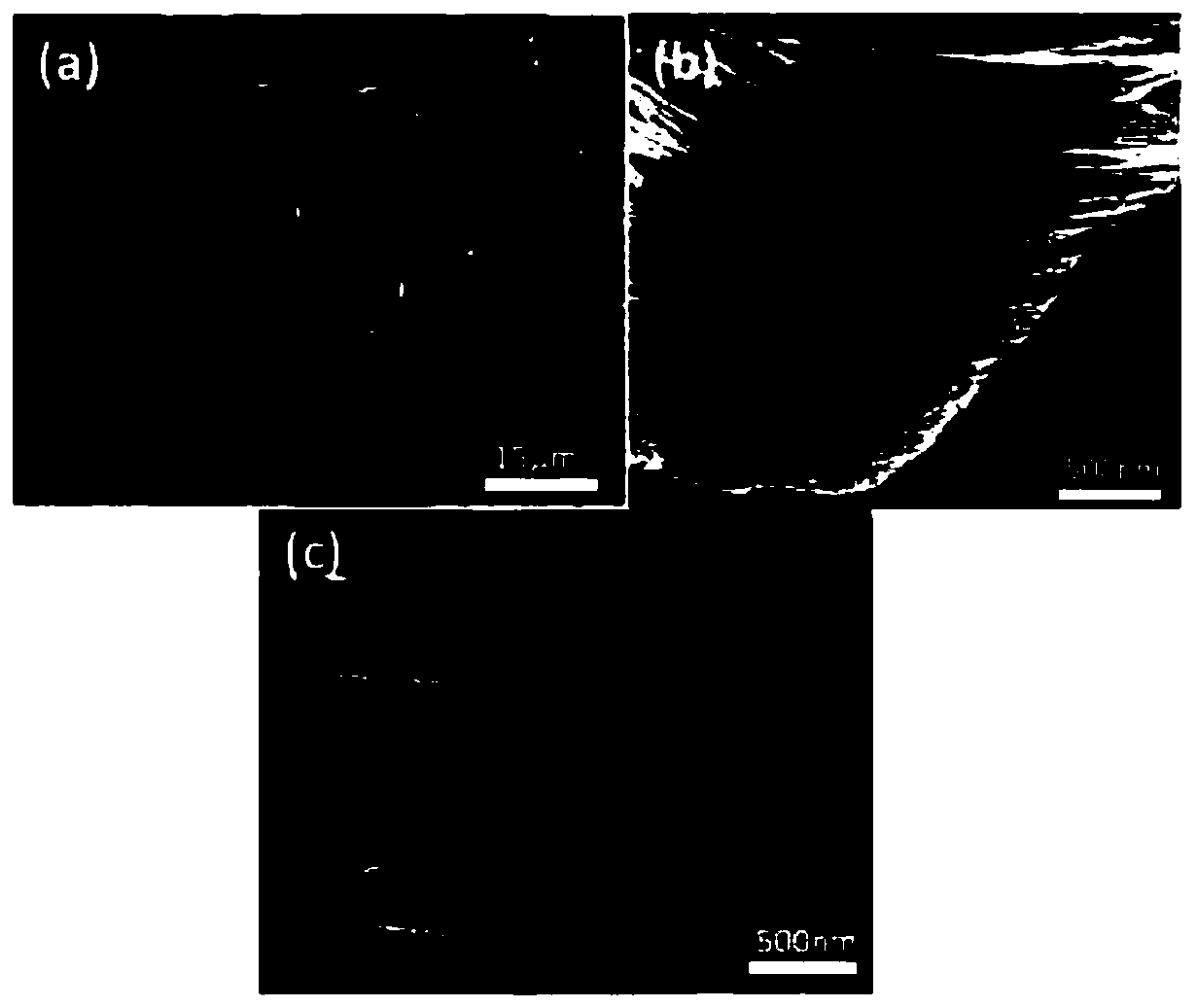
[0029] Step 4: Use a dropper to drop the black liquid onto the substrate and dry it to obtain Ti 3 C 2 ene film material.

Embodiment 2

[0031] Electromagnetic shielding electrode material Ti 3 C 2 The preparation method of ene film specifically comprises the following steps:

[0032] Step 1: Take 6mol / L HCL solution;

[0033] Step 2: Add 1.98g of LiF to it;

[0034] Step 3: Mix 3g of Ti in 10 minutes 3 AlC 2 added to the solution;

[0035] Step 4: Heating at 40°C for 42 hours, then cooling to room temperature naturally.

[0036] Step 5: Prepare the obtained black liquid, and wash it several times with deionized water repeatedly to remove the remaining reaction reagents.

[0037] Step 6: Use a dropper to drop the black liquid onto the substrate and dry it to obtain Ti 3 C 2 ene film material.

Embodiment 3

[0039] A method for preparing an anti-electromagnetic interference resistive variable memory, specifically comprising the following steps:

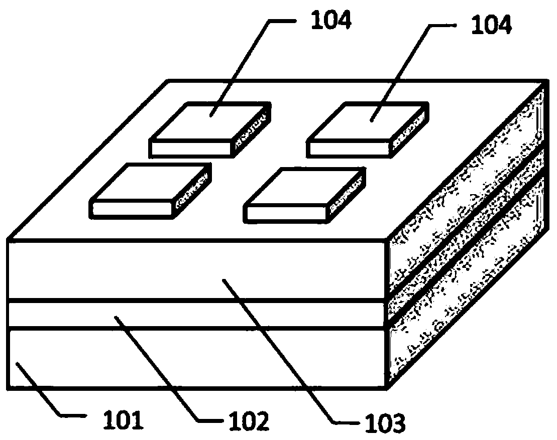
[0040] (1) Transfer Ti on the base material 3 C 2 ene film material, Ti 3 C 2 The preparation method of the ene film material uses one of the methods in Example 1 or Example 2.

[0041] (2) Using magnetron sputtering technology on Ti 3 C 2 Deposit storage function layer thin film material HfO on the ene thin film material 2 , the specific process is as follows: the background vacuum is 5×10 -5 Pa, working pressure 2Pa, Ar gas flow 20sccm, RF power 60W, deposition time 40min, HfO 2 The film thickness is 30nm.

[0042] (3) in HfO 2 Ti transfer on thin film surface 3 C 2 ene film material, Ti 3 C 2 The preparation method of the ene film material uses one of the methods in Example 1 or Example 2.

[0043] (4) On the top layer Ti 3 C 2 A layer of photoresist is suspended on the surface of the ene film material, and exposed to l...


PUM


Abstract

The invention discloses an anti-electromagnetic interference resistive memory and a preparation method thereof, which belong to the technical field of microelectronics. The resistive variable memory is a sandwich structure consisting of three layers of thin films, including a bottom electrode layer, a resistive variable functional layer and a top electrode layer, and the bottom electrode and top electrode layer are made of electromagnetic shielding material Ti 3 C 2 ene thin film, the resistive switching functional layer is an oxide material. The invention also discloses a preparation method of the resistive variable memory which is resistant to electromagnetic interference. The present invention selects Ti which is conductive, highly efficient electromagnetic shielding, and cheap and easy to obtain. 3 C 2 The ene thin film is used as an electrode material, and the resistive variable memory prepared has the advantages of light weight, high strength, and simple process, and meets the demand for portable and wearable electronic devices.

Description

technical field [0001] The invention belongs to the technical field of microelectronics, and in particular relates to an anti-electromagnetic interference resistive memory and a preparation method thereof. Background technique [0002] Electronic devices such as mobile phones and computers are becoming more and more portable and intelligent, and electronic components are running faster and faster. In the process of transmitting signals and utilizing electric energy of these electronic devices, electromagnetic waves will cause electromagnetic interference to electronic components, affecting the performance and service life of the equipment, accelerating the generation of waste electronic devices, polluting the surrounding environment, and detrimental to human health. An effective solution is to use effective electromagnetic shielding materials, on the one hand to reduce ineffective electromagnetic emissions, and on the other hand to protect devices from external signal interf...

Claims


Application Information

Patent Timeline
Patent Type & Authority Patents(China)
IPC IPC(8): H01L45/00H01L23/552
CPCH01L23/552H10N70/841H10N70/011
Inventor 赵鸿滨屠海令魏峰杨志民张国成
Owner GRIMAT ENG INST CO LTD
Why Eureka
Try Eureka