Preparing method for field effect electro-catalysis hydrogen production device
An electrocatalysis and field effect technology, applied in the field of nanomaterials and electrochemistry, can solve the problems of rare research on the influence of catalytic reactions, and achieve the effect of optimizing the electrocatalytic performance of nanomaterials, accurate testing and characterization, and optimizing the catalytic performance of materials
- Summary
- Abstract
- Description
- Claims
- Application Information
AI Technical Summary
Problems solved by technology
Method used
Image
Examples
Embodiment 1
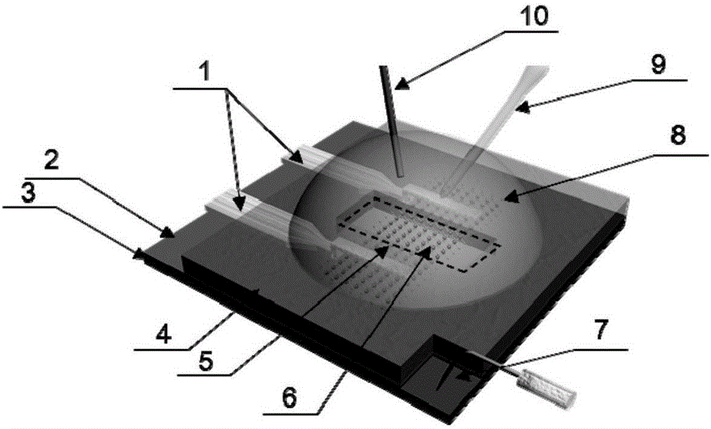
[0025] The preparation method of the field effect electrocatalytic hydrogen production device of the present invention, it comprises the steps:
[0026] 1) VSe prepared by mechanical exfoliation 2 The nano flakes 6 are dispersed onto a clean silicon substrate 3 with an oxide layer (the oxide layer is 300nm SiO 2 layer) surface, where the nanoflakes serve as the channel material, and the oxide layer serves as the dielectric layer 2.
[0027] 2) Metal microelectrodes arranged in parallel on both ends of the nanosheet 6 are fabricated as the working electrode 1 (Cr 5nm, Au 150nm) by means of electron beam exposure etching and physical thermal evaporation deposition.
[0028] 3) Spin-coat a layer of polymethyl methacrylate (PMMA) (thickness 1.6 μm) as the insulating layer 4, and use electron beam exposure and etching to etch a rectangular window parallel to the metal microelectrode at the position of the nanosheet 5. The channel material is exposed and the metal electrodes are c...
Embodiment 2
[0034] The method for testing the electrocatalytic performance optimization mechanism of nanosheets in the present invention, it comprises the steps:
[0035] 1) Select a clean heavily doped silicon substrate 3, and deposit 80nm Al on its surface using an atomic layer deposition system 2 o 3 as the dielectric layer 2.
[0036] 2) VSe prepared by mechanical exfoliation 2 The nano flakes 6 are dispersed on the surface of the silicon substrate 3 with an oxide layer.
[0037] 3) using electron beam exposure etching and physical thermal evaporation deposition on both ends of the nanosheet 6 (in contact with the nanosheet) and the outer side (not in contact with the nanosheet) and one side edge of the silicon substrate (the area where the oxide layer is removed) Metal microelectrodes (Cr 5nm, Au 150nm) were fabricated as the working electrode 1, the counter electrode 10 and the back gate electrode 7 respectively.
[0038] 4) Spin-coat a layer of PMMA with a thickness of 1.6 μm a...
Embodiment 3
[0045] In the present invention, the method for in-situ testing the influence of ion distribution on the electrical transport properties of materials in the electrocatalytic process of nanosheets comprises the following steps:
[0046] 1) VSe prepared by mechanical exfoliation 2 Nanoflakes 6 are dispersed onto a clean silicon substrate 3 with an oxide layer 2 (the surface is 300nm SiO 2 layer) surface, where the nanoflakes serve as the channel material, and the oxide layer serves as the dielectric layer 2.
[0047] 2) Metal microelectrodes 1 (Cr 5nm, Au 150nm) arranged in parallel are fabricated on both ends of the nanosheet 6 by means of electron beam exposure etching and physical thermal evaporation deposition.
[0048] 3) Spin-coat a layer of PMMA with a thickness of 1.6 μm as the insulating layer 4, and use electron beam exposure and etching to etch a rectangular window 5 parallel to the metal microelectrode at the position of the nanosheet 6, so that the channel material i...
PUM
 Abstract
Description
Claims
Application Information
 - R&D Engineer
- R&D Manager
- IP Professional
- Industry Leading Data Capabilities
- Powerful AI technology
- Patent DNA Extraction
Browse by: Latest US Patents, China's latest patents, Technical Efficacy Thesaurus, Application Domain, Technology Topic, Popular Technical Reports.
© 2024 PatSnap. All rights reserved.Legal|Privacy policy|Modern Slavery Act Transparency Statement|Sitemap|About US| Contact US: help@patsnap.com


