Carrying device and semiconductor processing equipment

A carrier device and processing technology, which is applied in the manufacture of semiconductor/solid-state devices, electrical components, circuits, etc., can solve the problems of uniform etching rate and uneven etching rate at the edge of the wafer, etc., to improve process uniformity, The effect of uniform etching rate

Active Publication Date: 2017-03-29
BEIJING NAURA MICROELECTRONICS EQUIP CO LTD
View PDF5 Cites 5 Cited by
  • Summary
  • Abstract
  • Description
  • Claims
  • Application Information

AI Technical Summary

Problems solved by technology

[0005] Because the above-mentioned focus ring 13 is processed by a single and uniform material, the impedance of its circumferential direction is the same everywhere, which makes the influence of the focus ring 13 circumferential direction on the electric field of the lower electrode also the same. However, in practice In applications, there are often cases where the etching rate at the edge of the wafer is not uniform, and the existing focus ring 13 does not have the ability to make the etching rate at the edge of the wafer tend to be uniform

Method used


Image

  • Carrying device and semiconductor processing equipment
  • Carrying device and semiconductor processing equipment
  • Carrying device and semiconductor processing equipment

Examples


Embodiment Construction

[0028] In order for those skilled in the art to better understand the technical solutions of the present invention, the carrying device and semiconductor processing equipment provided by the present invention will be described in detail below in conjunction with the accompanying drawings.

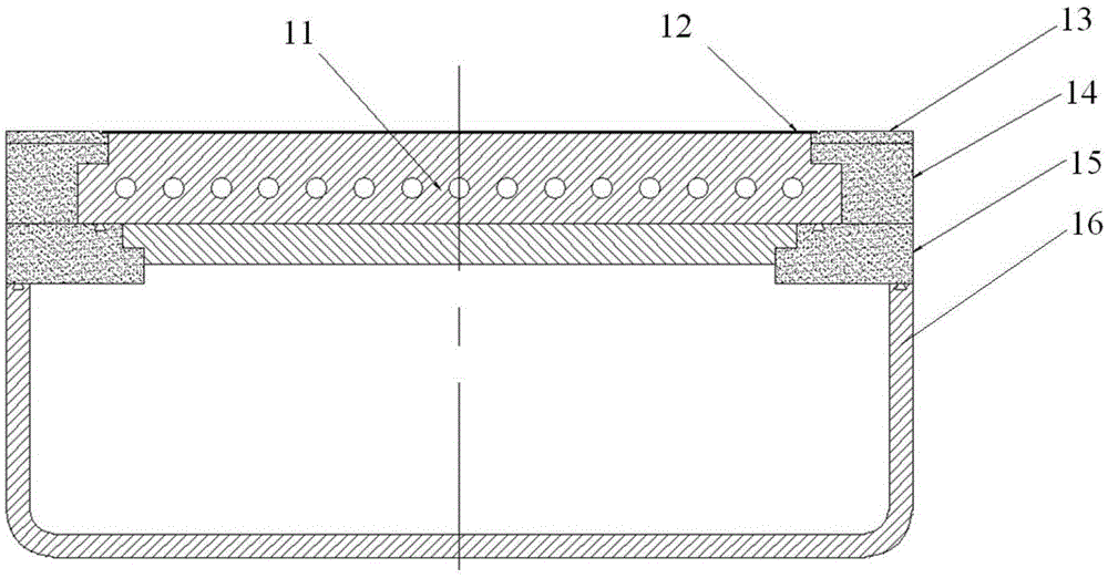
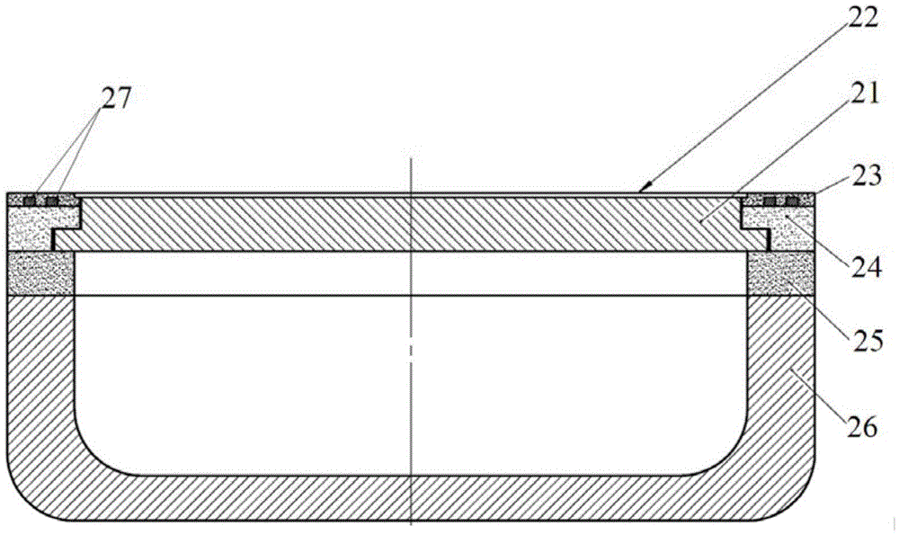
[0029] The carrying device provided by the present invention includes a chuck and a focus ring, the upper surface of the chuck is used to carry a workpiece to be processed, and the workpiece to be processed may be a wafer or a tray capable of carrying multiple wafers. The focus ring surrounds the outer periphery of the chuck, and the dielectric constant values ​​of different areas of the focus ring are different in the circumferential direction, so that the etching rate at the edge of the workpiece to be processed tends to be uniform.

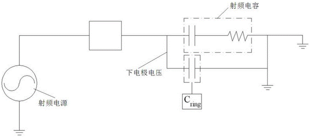
[0030] Further, figure 2 An equivalent circuit diagram of the lower electrode used for the carrying device used in this embodiment. see figure 2 , the c...


PUM


Abstract

The invention provides a carrying device and semiconductor processing equipment. The carrying device comprises a chuck and a focusing ring, wherein the upper surface of the chuck is used for carrying a processed workpiece; the focusing ring encircles the periphery of the chuck; and moreover, the dielectric constant values of the focusing ring at different areas in the peripheral direction are different, so that the etching rate of the edge of the processed workpiece everywhere tends to be uniform. According to the carrying device provided by the invention, the etching rate of the edge of the processed workpiece everywhere can tend to be uniform, so that the technological uniformity can be improved.

Description

technical field [0001] The invention relates to the field of semiconductor equipment manufacturing, in particular to a carrying device and semiconductor processing equipment. Background technique [0002] In the process of manufacturing integrated circuits (IC) and microelectromechanical systems (MEMS), especially in the process of implementing plasma etching (ETCH), physical vapor deposition (PVD), chemical vapor deposition (CVD), etc., often Use the supporting device to carry and heat the processed workpiece such as the wafer, provide DC bias voltage for the wafer and control the temperature of the wafer surface. [0003] figure 1 It is a schematic diagram of the structure of a typical bearing device. like figure 1 As shown, the carrier device includes an electrostatic chuck 11 and an edge assembly. Wherein, the electrostatic chuck 11 is used to fix the wafer 12 on its upper surface by means of electrostatic adsorption, and the electrostatic chuck 11 is also made of co...

Claims


Application Information

Patent Timeline
Patent Type & Authority Applications(China)
IPC IPC(8): H01L21/683H01L21/67
CPCH01L21/67011H01L21/6831
Inventor 郑友山成晓阳
Owner BEIJING NAURA MICROELECTRONICS EQUIP CO LTD
Why Eureka
Try Eureka