
Simulation design method for AC coupling capacitor reference plane

A technology of coupling capacitance and simulation design, applied in computing, electrical digital data processing, special data processing applications, etc., can solve problems such as impedance discontinuity, affecting link performance, affecting signal link insertion loss, etc., to ensure continuous impedance High reliability, operability, and space-saving effect

Inactive Publication Date: 2017-03-22
ZHENGZHOU YUNHAI INFORMATION TECH CO LTD
View PDF2 Cites 10 Cited by
  • Summary
  • Abstract
  • Description
  • Claims
  • Application Information

AI Technical Summary

Problems solved by technology

The ideal coupling capacitor will completely filter out the DC component of the signal, but in actual circuit work, the capacitor has parasitic inductance. Each capacitor itself, the fan-out leads of the capacitor, and the layer-changing vias are impedance discontinuous point
[0004] Impedance mismatch will bring reflections, affecting the insertion loss (IL), return loss (RL), jitter (Jitter) and bit error rate (BER) of the entire signal link, and ultimately affect the performance of the entire link

Method used


Image

  • Simulation design method for AC coupling capacitor reference plane
  • Simulation design method for AC coupling capacitor reference plane
  • Simulation design method for AC coupling capacitor reference plane

Examples


Embodiment 1

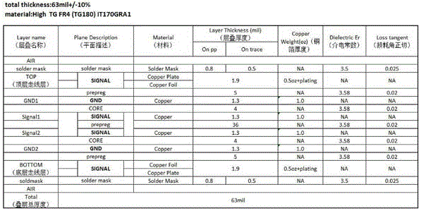
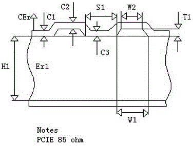
[0058] The simulated stackup adopts the attached figure 1 6-layer board shown, differential line impedance as attached figure 2 As shown, the capacitor is placed on the Top layer, referring to the GND of the second layer and the first reference layer. Hollow out the L2_GND first reference layer under the capacitor pad, and the capacitor pad will refer to the L3_first dielectric layer.

[0059] The capacitance information selected for simulation is as follows:

[0060] Capacitor size: 0402

[0061] Pad size: 18X22mil

[0062] Capacitor value: 0.01uf

[0063]Digging hole size: larger than the pad and so on, gradually increase by 2mil until the bottom of the capacitor is hollowed out as a whole.

[0064] Differential line impedance: 85ohmPCIE

[0065] Tracewidth: 8.3mil

[0066] TraceSpacing: 5.7mil

[0067] The emulation scheme that the present invention adopts is:

[0068] Construct the PCB model, use Sigrity PowerSI to extract the PCBS parameters, and then import the...

Embodiment 2

[0090] Further, a printed circuit board PCB includes a GND first reference layer, a GND second reference layer, a first dielectric layer, a second dielectric layer, a Top layer and a Bottom layer, and a signal transmission link, and the signal The transmission link is installed on the Top layer;

[0091] Wherein, the signal transmission link includes: two transmission lines and an alternating current AC coupling capacitor module, wherein the two transmission lines are connected through the AC coupling capacitor module;

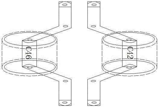
[0092] The GND first reference layer is provided with an impedance hole, and the opening area of ​​the impedance hole is enlarged by 4mil for the projection area of ​​the AC coupling capacitor module projected on the GND first reference layer in a positive projection mode. The shape of the aperture area is a longitudinal ellipse.

[0093] The signal transmission link includes: two transmission lines and an AC coupling capacitor module, wherein the two transmi...


PUM


Abstract

The invention discloses a simulation design method for an AC coupling capacitor reference plane. The method comprises the steps of S1, establishing a PCB model, wherein a hole digging size of an impedance hole is gradually increased by 2mil from a size equal to that of a pad, until the lower side of a capacitor is integrally hollowed; S2, extracting a PCB S parameter through utilization of Sigrity Power SI, importing the S parameter into Hspice for TDR impedance simulation, thereby obtaining a TDR impedance simulation curve and the TDR impedance simulation curve at the position of the capacitor; S3, extracting the impedance at the position of 470ps, obtaining impedance values corresponding to 7 cases and drawing an impedance change curve; and S4, analyzing a simulation result. The method has the beneficial effects that 1, through comparison of various elliptical hole digging modes, a hole digging area with the best impedance continuity effect is found, the impedance continuity of a link is ensured, thereby achieving a signal completeness purpose; and 2, the elliptical hole digging size is researched, thereby obtaining the best hoe digging area, the method is high in operability, is easy to realize in design and production and can be widely applied to the field of high-speed PCB design.

Description

technical field [0001] The invention relates to the field of high-speed PCB design, in particular to a simulation design method of an AC coupling capacitor reference plane. Background technique [0002] In today's era, Internet technology is developing rapidly, and information technology is changing rapidly every day. With the advent of the cloud era and the era of big data, the amount of network data has increased explosively. The transmission of massive data not only poses a test for network transmission equipment, but also for High-speed signal transmission rate puts forward higher requirements. [0003] As data rates increase, small impedance discontinuities on high-speed serial links can cause signal reflections, crosstalk, mode switching, and other adverse effects. There are usually AC coupling capacitors connected in series on the SERDES serial signal differential link to filter out the DC component of the high-speed signal. The ideal coupling capacitor will complet...

Claims


Application Information

Patent Timeline
Patent Type & Authority Applications(China)
IPC IPC(8): G06F17/50
CPCG06F30/367G06F30/398
Inventor 刘强进张长林
Owner ZHENGZHOU YUNHAI INFORMATION TECH CO LTD
Learn More