
Photo-curable resin composition

A technology of photocurable resin and composition, which is applied in the field of photocurable resin composition, can solve the problem of cost, limitation of fine pattern formation, long time-consuming and other problems, and achieve excellent coating property, fast photocuring, saving The effect of investment fees

Active Publication Date: 2017-02-22
DONGJIN SEMICHEM CO LTD
View PDF5 Cites 4 Cited by
  • Summary
  • Abstract
  • Description
  • Claims
  • Application Information

AI Technical Summary

Problems solved by technology

[0002] In conventional photolithography, which is used to realize fine patterns in the LCD process or semiconductor process for manufacturing displays, the circuit line width (or pattern line width) depends on the wavelength of light used in the exposure process. Material and equipment technology, fine pattern formation is subject to many restrictions
In addition, each time a pattern is formed, exposure, post-exposure bake, development, post-development bake, etching, and washing steps need to be performed, so there is a problem that it takes a long time and the process is very complicated.
In addition, an expensive exposure instrument is used to improve performance, so cost is also a problem

Method used


Image

  • Photo-curable resin composition
  • Photo-curable resin composition
  • Photo-curable resin composition

Examples


Embodiment 1 to 3 and comparative example 1

[0048] According to the composition of the following Table 1, each component was mixed, and it mixed uniformly at normal temperature for 6 hours or more, and the resin composition (unit: weight part) was manufactured.

[0049] At this time, the components used are as follows.

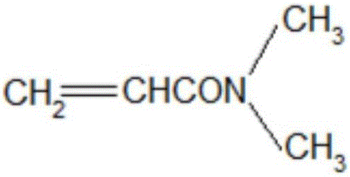
[0050] Acrylamide monomer: acryloyl morpholine (ACMO, Acryloyl morpholine, manufactured by Japan Kyojin Company) of chemical formula 1, dimethylacrylamide (DMAA, N, N-Dimethyl acrylamide, manufactured by Japanese Kyojin Company) of chemical formula 2;

[0051] Acrylic copolymer resin: (polyester acrylate (PS420, Tetrafunctional Polyester acrylate, Korea Miwon Specialty Chemical Company);

[0052] Vinyl monomer: (glycidyl methacrylate (GMA, Glycidyl metaacrylate, Sigma-Aldrich);

[0053] Cross-linking monomers: pentaerythritol triacrylate (PETA, Pentaerythritol triacrylate, Korea Miwon Specialty Chemical Company), 1,4-butanediol diacrylate (HDDA, 1,4-butandioldiacrylate, Korea Miwon Specialty Chemical C...


PUM


Abstract

The present invention relates to a photo-curable resin composition and, more particularly, to a photo-curable resin composition for forming micro patterns, the photo-curable resin composition being applicable to a flexible display substrate since the composition can be cured at high speed and has excellent coating properties, adhesive properties and acid resistance by virtue of comprising acrylamide monomer.

Description

technical field [0001] The present invention relates to a photocurable resin composition. More specifically, it relates to a photocurable resin composition that can achieve rapid curing and is excellent in applicability, adhesiveness, and acid resistance by including an acrylamide monomer. Background technique [0002] In the conventional photolithography method used to realize fine patterns in the LCD process or semiconductor process for manufacturing displays, the circuit line width (or pattern line width) depends on the wavelength of light used in the exposure process. There are many limitations in material and equipment technology and fine pattern formation. In addition, exposure, post-exposure bake, development, post-development bake, etching, washing steps, and the like need to be performed every time a pattern is formed. Therefore, there is a problem that it takes a long time and the process is very complicated. In addition, since an expensive exposure instrument and...

Claims


Application Information

Patent Timeline
IPC IPC(8): C08F265/06C08F290/06C08F220/56
Inventor 宋晙溶申承协崔美镜智锡焕崔俊浩金龙宇
Owner DONGJIN SEMICHEM CO LTD
Learn More