Back technique for semiconductor ultrathin device

A backside technology, semiconductor technology, applied in the direction of semiconductor devices, semiconductor/solid-state device manufacturing, electric solid-state devices, etc., to achieve the effect of high technology maturity and good market application prospects

Active Publication Date: 2017-02-22
NO 55 INST CHINA ELECTRONIC SCI & TECHNOLOGYGROUP CO LTD
View PDF3 Cites 2 Cited by
  • Summary
  • Abstract
  • Description
  • Claims
  • Application Information

AI Technical Summary

Problems solved by technology

[0005] However, there are few related reports on the crack control technology in the process of ultra-thin wafer cleaning and on-wafer testing after debonding ultra-thin wafers before wafer dicing.

Method used


Image

  • Back technique for semiconductor ultrathin device
  • Back technique for semiconductor ultrathin device
  • Back technique for semiconductor ultrathin device

Examples


Embodiment Construction

[0028] A back process method for semiconductor ultra-thin devices, comprising the following steps:

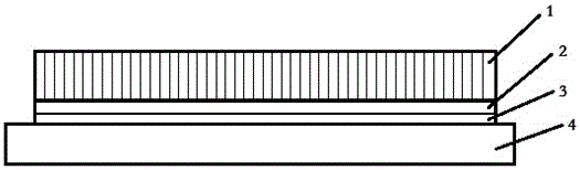
[0029] 1) Wafer bonding: The semiconductor wafer 1 coated with high-temperature bonding agent 2 on the front side is bonded to the first carrier 4 coated with low-temperature bonding agent 3. The bonded structure is as follows figure 1 shown;

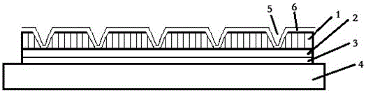
[0030] 2) Backside process: the wafer in step 1) is thinned into an ultra-thin sheet, and then conventional backside processes such as backside through holes and backside metallization are completed in sequence. After the conventional backside process is completed, the structure is as follows figure 2 shown;

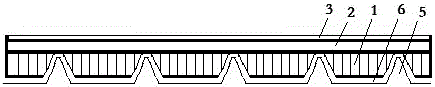
[0031] 3) Wafer separation: After completing step 2), the low-temperature bonding agent 3 is softened by thermal separation to realize the separation of the ultra-thin wafer from the first carrier 4. The structure of the ultra-thin wafer after separation is as follows image 3 shown;

[0032] 4) The secondary attachment carrier...


PUM


Abstract

The invention discloses a back technique for a semiconductor ultrathin device. The technique comprises the main steps of (1) bonding a wafer of which the surface is coated with a high-temperature bonding agent and a first carrier coated with a low-temperature bonding agent; (2) thinning the wafer into an ultrathin wafer and then sequentially completing conventional back processes of a back through hole, back metallization and the like; (3) separating the ultrathin wafer from the first carrier; (4) attaching the ultrathin wafer to a second carrier and then cleaning and removing the high-temperature bonding agent and the low-temperature bonding agent; (5) separating the ultrathin wafer from the second carrier; (6) carrying out an electric performance test on the ultrathin wafer on a third carrier; and (7) attaching the ultrathin wafer to the second carrier and carrying out wafer cutting. The technique has the advantages that (1) the ultrathin wafer is supported by the carriers in the back process, reduction of the split ratio of the ultrathin wafer in the back process is facilitated and the yield of the process is improved; and (2) the used carriers all are regular-size carriers of a semiconductor, the process is suitable for massive production of the device and the technique maturity is high. The technique has a good market application prospect.

Description

technical field [0001] The invention relates to a manufacturing method of a semiconductor device, in particular to a back processing method for a semiconductor ultra-thin device, and the method is suitable for processing the back of an ultra-thin sheet in the manufacturing process of an ultra-thin power device. Background technique [0002] In the manufacturing process of semiconductor devices, in order to obtain better mechanical properties, electrical properties, and the needs of subsequent processing technology, it is generally necessary to reduce the thickness of the product sheet, which is generally reduced to less than 200 microns, which is called a thin sheet. For some special semiconductor devices, especially some power semiconductor devices, in order to obtain thinner chips, or to meet the requirements of better electrical performance, it is necessary to reduce the thickness of the product sheet to less than 100 microns, or even less than 50 microns, that is, It is ...

Claims


Application Information

Patent Timeline
IPC IPC(8): H01L21/683
CPCH01L21/6835H01L2221/68327H01L2221/6834
Inventor 邹鹏辉王彦硕高建峰黄念宁李信赵玲陈元坤
Owner NO 55 INST CHINA ELECTRONIC SCI & TECHNOLOGYGROUP CO LTD
Why Eureka
Try Eureka