Array substrate, manufacturing method of routing line and test pad of array substrate as well as liquid crystal panel

A technology of an array substrate and a manufacturing method, which is applied in the field of liquid crystal display, can solve the problems of damage to devices, easy accumulation of large charges, easy occurrence of electrostatic discharge, etc., and achieves the effects of reducing electrostatic discharge, reducing the probability of occurrence, and reducing parasitic capacitance

Inactive Publication Date: 2017-02-15
SHENZHEN CHINA STAR OPTOELECTRONICS TECH CO LTD
View PDF3 Cites 3 Cited by
  • Summary
  • Abstract
  • Description
  • Claims
  • Application Information

AI Technical Summary

Problems solved by technology

However, in the existing wiring structure, there is only a very thin layer of the first metal layer (which is formed simultaneously with the gate metal layer) and the second metal layer (which is formed simultaneously with the source-drain metal layer). An insulating layer (which is formed at the same time as the gate insulating layer), and a large amount of charge is easy to accumulate between the first metal layer and the second metal layer, so that electrostatic discharge is very easy to occur, and then damage the device

Method used


Image

  • Array substrate, manufacturing method of routing line and test pad of array substrate as well as liquid crystal panel
  • Array substrate, manufacturing method of routing line and test pad of array substrate as well as liquid crystal panel
  • Array substrate, manufacturing method of routing line and test pad of array substrate as well as liquid crystal panel

Examples


Embodiment Construction

[0026] Hereinafter, embodiments of the present invention will be described in detail with reference to the accompanying drawings. The present invention may, however, be embodied in many different forms and should not be construed as limited to the specific embodiments set forth herein. Rather, these embodiments are provided to explain the principles of the invention and its practical application, to thereby enable others skilled in the art to understand the invention for various embodiments and with various modifications as are suited to the particular intended use.

[0027] In the drawings, the thickness of layers and regions are exaggerated for clarity of the device. The same reference numbers refer to the same elements throughout the drawings.

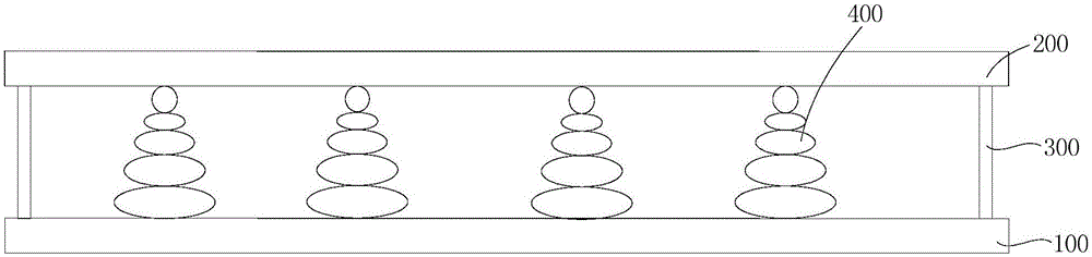
[0028] figure 1 A schematic diagram of a structure of a liquid crystal panel according to an embodiment of the present invention.

[0029] refer to figure 1 The liquid crystal panel according to the embodiment of the present inv...


PUM


Abstract

The invention provides an array substrate. The array substrate comprises a test pad located in a test pad area and a routing line located in a routing area, wherein the routing line is connected with the test pad; the routing line comprises a first metal layer, a first insulation layer, a first passivation layer, a second insulation layer, a second passivation layer and a transparent electrode layer which are successively arranged on the substrate and are located in the routing area. The invention also provides a manufacturing method of the routing line and the test pad of the array substrate as well as a liquid crystal panel. In a routing structure of the array substrate, a second metal layer which is a source-drain metal layer of a thin film transistor is eliminated; a pixel electrode layer is in span connection with the first metal layer; a plurality of film layers are arranged between the pixel electrode layer and the first metal layer, and a long distance is formed between the pixel electrode layer and the first metal layer, thus the breakdown threshold voltage can be increased, and the stray capacitance can be reduced, so that the occurrence probability of electrostatic discharge can be reduced.

Description

technical field [0001] The invention belongs to the technical field of liquid crystal display, and in particular, relates to an array substrate, a manufacturing method of its wiring and test pads, and a liquid crystal panel. Background technique [0002] With the evolution of optoelectronic and semiconductor technology, it has also led to the vigorous development of Flat Panel Display. Among many flat panel displays, Liquid Crystal Display (LCD) has high space utilization efficiency, low power consumption, Many superior features such as no radiation and low electromagnetic interference have been used in all aspects of production and life. [0003] A liquid crystal display usually includes a liquid crystal panel and a backlight module arranged opposite to each other. Since the liquid crystal panel cannot emit light, the backlight module needs to provide uniform light to the liquid crystal panel, so that the liquid crystal panel can display images. A liquid crystal panel gene...

Claims


Application Information

Patent Timeline
Patent Type & Authority Applications(China)
IPC IPC(8): G02F1/1362G02F1/1368
CPCG02F1/136286G02F1/1368G02F2202/22G02F1/136254
Inventor 王勐
Owner SHENZHEN CHINA STAR OPTOELECTRONICS TECH CO LTD
Why Eureka
Try Eureka