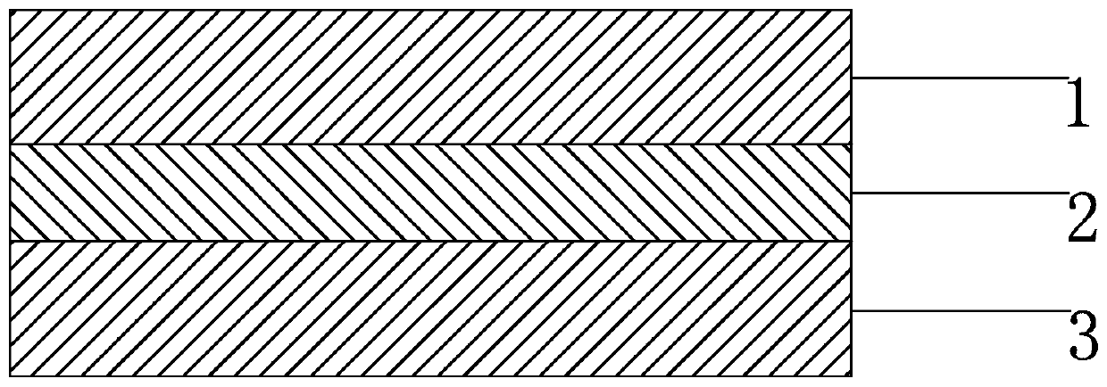
Low driving voltage dimming film and preparation method thereof
A technology of low driving voltage and dimming film, which is applied in the field of dimming film, can solve the problems that the transmittance cannot reach the best and the safety voltage cannot be reached, and achieve excellent photoelectric performance, strong shielding, and long service life. Effect
- Summary
- Abstract
- Description
- Claims
- Application Information
AI Technical Summary
Problems solved by technology
Method used
Image
Examples
specific Embodiment approach 1
[0034] Step a, in a light-shielding environment, mix isobornyl acrylate 25%, isobornyl methacrylate 39%, methacrylate 3%, methacrylate-2-hydroxyethyl 8%, acrylic acid 21%, silane 1% of the joint agent and 3% of 2,4,6-(trimethylbenzoyl) diphenylphosphine oxide are mixed in proportion, and after mixing, they are fully stirred evenly to obtain UV optical adhesive A;
[0035] Step b, mix 40% of UV optical glue with 60% of HPC854200-100 liquid crystal and stir well to obtain mixture B;
[0036] Step c, add 5‰ of 20μm spacers and mix with B, stir well and evenly after defoaming to obtain the final PDLC, waiting for coating construction;
[0037] Step d, the PDLC is sandwiched between two transparent nano-silver conductive films, and rolled to form a liquid crystal film; wherein the nano-silver conductive film is 125 microns thick, with a square resistance of 50Ω, a total light transmittance of 87%, and a haze of 0.8 %;
[0038] Step E, UV curing the liquid crystal film, wherein th...
specific Embodiment approach 2
[0042] Step a, in a light-shielding environment, mix 60% isobornyl methacrylate, 3% hydroxyalkyl methacrylate, 3% 2-hydroxyethyl methacrylate, 26% methacrylic acid, lauryl methacrylate 3% of ester, 2% of silane coupling agent, 3% of 2,4,6-(trimethylbenzoyl) diphenylphosphine oxide are mixed in proportion, and fully stirred evenly after mixing to obtain UV optical adhesive A;
[0043] Step b, mix 45% of UV optical glue with 55% of SLC1717 liquid crystal and stir well to obtain mixture B;
[0044] Step c, add 4‰ of 20μm spacers and mix with B, stir well and evenly after degassing to obtain the final PDLC, waiting for coating construction;
[0045] Step d, the PDLC is sandwiched between two transparent ITO conductive films, and rolled to form a liquid crystal film; wherein the thickness of the ITO conductive film is 188 microns, the square resistance is 50Ω, the total light transmittance is 85%, and the haze is 0.9%;
[0046] Step E, UV curing the liquid crystal film, wherein th...
PUM
| Property | Measurement | Unit |
|---|---|---|
| diameter | aaaaa | aaaaa |
| electrical resistance | aaaaa | aaaaa |
| electrical resistance | aaaaa | aaaaa |
Abstract
Description
Claims
Application Information
 - R&D Engineer
- R&D Manager
- IP Professional
- Industry Leading Data Capabilities
- Powerful AI technology
- Patent DNA Extraction
Browse by: Latest US Patents, China's latest patents, Technical Efficacy Thesaurus, Application Domain, Technology Topic, Popular Technical Reports.
© 2024 PatSnap. All rights reserved.Legal|Privacy policy|Modern Slavery Act Transparency Statement|Sitemap|About US| Contact US: help@patsnap.com


