Radio frequency multi-chip circuit electromagnetic shielding structure

A technology of electromagnetic shielding structure and electromagnetic interference shielding, applied in circuits, electrical components, electrical solid devices, etc., can solve problems such as unfavorable high-density packaging

Inactive Publication Date: 2017-01-04
STATE GRID LIAONING ELECTRIC POWER RES INST +3
View PDF4 Cites 5 Cited by
  • Summary
  • Abstract
  • Description
  • Claims
  • Application Information

AI Technical Summary

Problems solved by technology

EMI shielding in the prior art is to shield the entire chip externally using a Faraday cage, and shield the chip in the entire package as a whole, which is not conducive to further high-density packaging

Method used


Image

  • Radio frequency multi-chip circuit electromagnetic shielding structure
  • Radio frequency multi-chip circuit electromagnetic shielding structure
  • Radio frequency multi-chip circuit electromagnetic shielding structure

Examples


Embodiment Construction

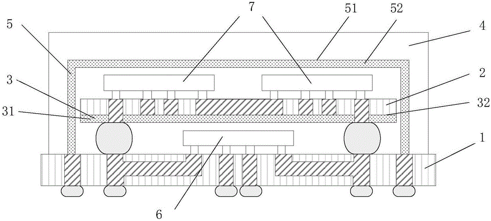
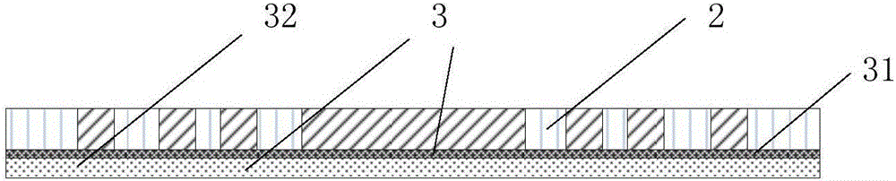
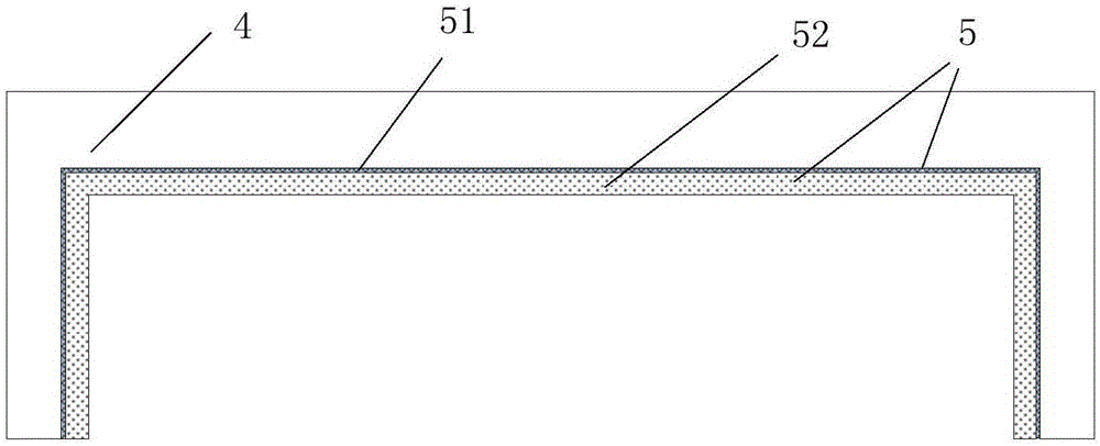
[0022] The specific embodiments of the present invention will be described in detail below with reference to the drawings, but it should be understood that the protection scope of the present invention is not limited by the specific embodiments.

[0023] In order to make the objectives, technical solutions, and advantages of the embodiments of the present invention clearer, the technical solutions in the embodiments of the present invention will be described clearly and completely in conjunction with the accompanying drawings in the embodiments of the present invention. Obviously, the described embodiments It is a part of the embodiments of the present invention, not all the embodiments. Based on the embodiments of the present invention, all other embodiments obtained by those of ordinary skill in the art without creative work shall fall within the protection scope of the present invention. Unless otherwise expressly stated otherwise, throughout the specification and claims, the ...


PUM


Abstract

The invention relates to a radio frequency multi-chip circuit electromagnetic shielding structure, and the structure comprises a substrate (1) and a substrate (2), which are connected. A substrate electromagnetic interference shielding layer (3) is attached to the lower surface of the substrate (2). The substrate (1), the substrate (2) and the substrate electromagnetic interference shielding layer (3) form a bottom first circuit assembly electromagnetic shielding structure. The housing (4) is disposed on the substrate (1), and a housing electromagnetic interference shielding layer (5) is attached to the internal surface of the housing (4). The substrate (2) is disposed in the housing (4). The substrate (2), the housing (4) and the housing electromagnetic interference shielding layer (5) form an upper second circuit assembly electromagnetic shielding structure. Therefore, the structure provided by the invention can achieve the internal and external electromagnetic shielding of a multi-chip high-density package at the same time.

Description

Technical field [0001] The invention relates to the technical field of integrated circuits, in particular to an electromagnetic shielding structure for radio frequency multi-chip circuits. Background technique [0002] Multi-chip package (English: Multi Chip Package, abbreviation: MCP) in package-on-package (English: Package-on-Package, abbreviation: PoP), designed to vertically integrate discrete logic and memory ball grid arrays (English: BallGrid Array) , Abbreviation: BGA) package. Stack the chips of the original discrete structure into the same package, and stack two or more chips into the same package, providing applications for communication equipment, navigation equipment, mobile phones, personal digital terminals, desktop computers, portable computers, tablet computers, etc. An ideal high-density packaging solution. [0003] Based on this, the inventors of the present invention found that the high-density package contains RF components, which requires electromagnetic int...

Claims


Application Information

Patent Timeline
IPC IPC(8): H01L23/552
CPCH01L2224/16225H01L23/552
Inventor 欧清海高强王峥李涛程大伟李良赵东艳曾令康于华东李温静
Owner STATE GRID LIAONING ELECTRIC POWER RES INST
Why Eureka
Try Eureka