Solar cell array, solar cell module and manufacturing method thereof
A technology for solar cells and solar cells, applied in the field of solar cells, can solve the problems of large resistance, long current path, affecting the photoelectric conversion efficiency of solar cell modules, etc., and achieve the effects of high efficiency, low cost, and high photoelectric conversion efficiency.
- Summary
- Abstract
- Description
- Claims
- Application Information
AI Technical Summary
Problems solved by technology
Method used
Image
Examples
preparation example Construction
[0128] During the preparation process of the solar cell module 100 , the conductive wire can be welded to the auxiliary grid line and the back electrode of the battery sheet 31 first, and then the various layers are stacked and laminated.
[0129] Other components of the solar cell assembly 100 according to the present application may be known in the art, and will not be repeated here.
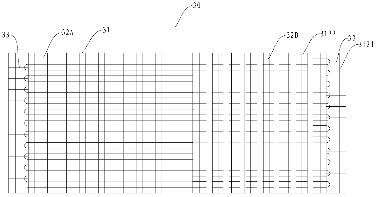
[0130] Specifically, the solar cell module 100 includes an upper cover plate 10 , a front adhesive film layer 20 , a cell array 30 , a rear adhesive film layer 40 and a back sheet 50 . The battery slice array 30 includes a plurality of battery slices 31, adjacent battery slices 31 are connected by a plurality of conductive wires 32, at least two conductive wires 32 are formed by metal wires S reciprocatingly extending between the surfaces of adjacent battery slices, The conductive wires 32 are welded to the auxiliary grid wires, and the front adhesive film layer 20 is in direct contact with th...
example 1
[0155] Example 1 is used to illustrate an example of the solar cell module 100 of the present application and its manufacturing method.
[0156] (1) Preparation of wire S
[0157] Attach a layer of Sn40%-Bi55%-Pb5% alloy layer (melting point is 125 ℃) on the surface of the copper wire, wherein the cross-sectional area of the copper wire is 0.04mm 2 , the thickness of the alloy layer is 16 μm, thereby making a wire S.
[0158] (2) Preparation of solar cell module 100
[0159] Provide a POE film layer with a size of 1630×980×0.5mm (melting temperature is 65°C), and accordingly provide a glass plate with a size of 1633×985×3mm and 60 pieces of polycrystalline silicon cells with a size of 156×156×0.21mm Tablet 31. The front side of the battery sheet 31 has 91 auxiliary grid lines (the material is silver, the width is 60 microns, and the thickness is 9 microns), each auxiliary grid line basically runs through the battery sheet 31 in the longitudinal direction, and between adja...
example 2
[0171] Example 2 is used to illustrate an example of the solar cell module of the present application and its preparation method.
[0172] (1) Preparation of wire S
[0173] Attach a layer of Sn40%-Bi55%-Pb5% alloy layer (melting point is about 125°C) on the surface of the copper wire, wherein the cross-sectional area of the copper wire is 0.03mm 2 , the thickness of the alloy layer is 10 μm, thereby producing a wire S.
[0174] (2) Preparation of solar cell modules
[0175] Provide an EVA film layer with a size of 1630×980×0.5mm (melting temperature is 60°C), a glass plate with a size of 1633×985×3mm and 60 pieces of polycrystalline silicon cells 31 with a size of 156×156×0.21mm. The light-receiving surface of the battery sheet 31 is provided with 91 auxiliary grid lines (the material is silver, the width is 60 microns, and the thickness is 9 microns), and each auxiliary grid line basically runs through the battery sheet 31 in the longitudinal direction, and two adjacent ...
PUM
 Abstract
Description
Claims
Application Information
 - R&D
- Intellectual Property
- Life Sciences
- Materials
- Tech Scout
- Unparalleled Data Quality
- Higher Quality Content
- 60% Fewer Hallucinations
Browse by: Latest US Patents, China's latest patents, Technical Efficacy Thesaurus, Application Domain, Technology Topic, Popular Technical Reports.
© 2025 PatSnap. All rights reserved.Legal|Privacy policy|Modern Slavery Act Transparency Statement|Sitemap|About US| Contact US: help@patsnap.com


