
Photoetching vacuum clamp for perforated ceramic chip of thin-film circuit

A thin-film circuit and vacuum clamp technology, applied in microlithography exposure equipment, optics, optomechanical equipment, etc., can solve the vacuum adsorption failure, affect the dimensional stability of high-frequency circuits, and cannot complete the matching of substrate and lithography patterns. To solve problems such as position work, to achieve the effect of convenient clamping, convenient gas path and sealing processing, and convenient clamping

Inactive Publication Date: 2016-11-23
10TH RES INST OF CETC
View PDF5 Cites 6 Cited by
  • Summary
  • Abstract
  • Description
  • Claims
  • Application Information

AI Technical Summary

Problems solved by technology

Because of the hole in the middle of the ceramic chip with holes, the vacuum hole on the surface of the adsorption fixture will leak air, so that the ceramic chip cannot be vacuum adsorbed and fixed by the vacuum equipment stage, and the vacuum adsorption will fail, and the alignment between the substrate and the photolithography plate cannot be completed Work
If adhesive tape is used to fix the ceramic workpiece, the first defect is that the thickness of the tape produces a gap that makes the edge of the exposed figure vignetting, which affects the dimensional stability of the high-frequency circuit; the second defect is that the tape is sandwiched between the ceramic chip and the photolithography plate as a protrusion, The high precision of graphics requires that the lithography machine adopts the hard contact mode. The lifting platform of the vacuum equipment will automatically raise the hard top photolithography plate of the ceramic workpiece. Since the thickness of the photolithography plate is much larger than that of the ceramic workpiece, it is the ceramic workpiece that is damaged.

Method used


Image

  • Photoetching vacuum clamp for perforated ceramic chip of thin-film circuit
  • Photoetching vacuum clamp for perforated ceramic chip of thin-film circuit
  • Photoetching vacuum clamp for perforated ceramic chip of thin-film circuit

Examples


Embodiment Construction

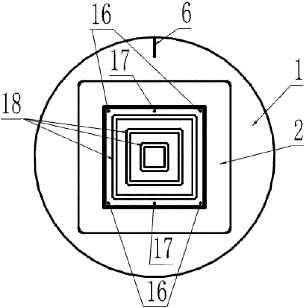
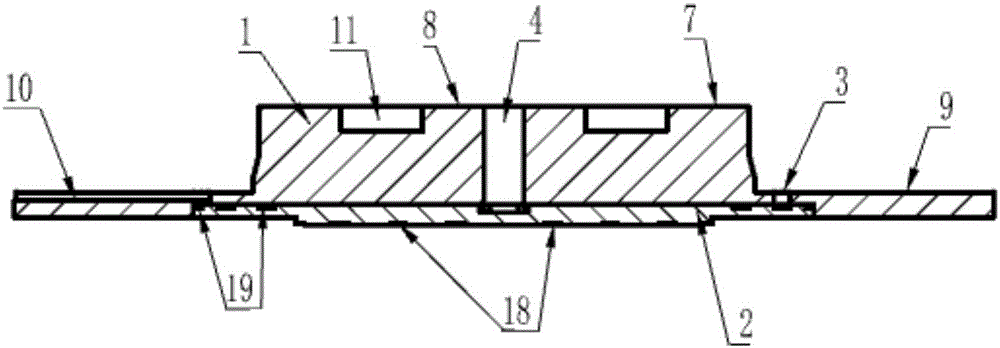
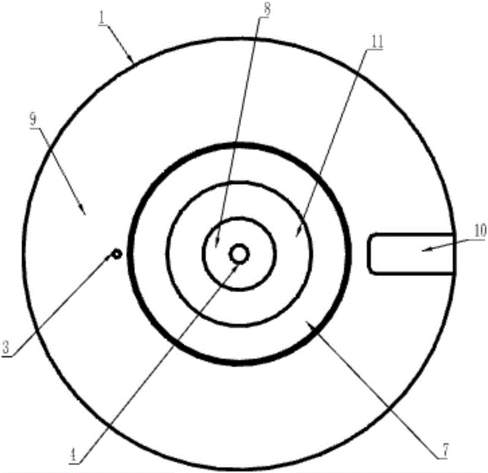
[0022] exist Figure 1-Figure 5 In the shown embodiment, a vacuum fixture for photolithography of a thin film circuit ceramic sheet with holes includes: an alignment shunt chassis 1 and its alignment marking line 6 located on the bisector of the circumferential angle, and the alignment shunt chassis 1 1. The adsorption table 2 in the lower end of the chassis is installed in the groove 5. The counter-distribution chassis 1 is formed with two circular planes consisting of three concentric circular platforms with different diameters. The center of the circular platform is formed with an air guide hole 4 and grooves 11 located on both sides of the air guide hole 4 and the adsorption surface 7 and sealing surface formed by it. 8, wherein the grooves 11 located on both sides of the air guide hole 4 form two air paths that are airtight with the vacuum equipment; the side of the adjacent root of the flange ring surface 9 connected to the concentric circle platform is provided with a mob...


PUM


Abstract

The invention discloses a photoetching vacuum clamp for a perforated ceramic chip of a thin-film circuit, and aims at providing a vacuum adsorption clamp which has the advantages that clamping is convenient, the universality is high, and the yield is high. According to the photoetching vacuum clamp, marked line endpoint vacuum absorption holes (17) which take an air guide hole (4) as the center and bypass the free ends of aligning marked lines (6) are perforated in an adsorption platform (2), and then an inner ring seal groove (12) of a rectangular ring groove is formed; the orthogonal air guide hole and crisscross air guide slots (14) which are overlapped and radiated with diagonal lines of the rectangular ring groove are perforated in the region of the inner ring seal groove, vacuum adsorption holes (16) are perforated in the four endpoints of the crisscross lines, a middle layer air guide groove (15) which is a ring groove formed by the moment structure at the roots of the aligning marked lines and an outer layer inner ring seal groove (13) which surrounds the middle layer air guide groove are perforated in the periphery of the inner ring seal groove (12), vacuum adsorption holes are distributed on the four corners of the bearing face of a ceramic chip workpiece and communicated with the crisscross air guide slots, and during the working process, the vacuum adsorption holes adsorb the four corners of the ceramic chip to fix the ceramic chip workpiece.

Description

technical field [0001] The invention relates to a thin-film circuit photolithography vacuum jig with holes, which is suitable for MJB4 automatic lithography vacuum equipment with different functions and two-way vacuum adsorption carrying platforms. Background technique [0002] In the manufacturing process of ceramic thin film circuit substrates, the design graphics are transferred to the coated ceramics, so as to achieve the synchronization of the design graphics and the product circuit graphics, and a process called photolithography is used to achieve the above purpose. The current method for photoetching thin film circuit patterns on ceramic substrates is to use UV-sensitive positive photoresist as a resist, and perform photolithographic imaging of thin film circuit patterns on the upper surface of ceramic substrates. After a series of follow-up processes, a ceramic thin film circuit is finally formed. The photolithography process includes three processes of gluing, phot...

Claims


Application Information

Patent Timeline
Patent Type & Authority Applications(China)
IPC IPC(8): G03F7/20
CPCG03F7/707
Inventor 詹为宇林晓莉
Owner 10TH RES INST OF CETC
Learn More