A two-dimensional chiral metal-medium nanostructure and its preparation method
A nanostructure and chiral technology, applied in the field of two-dimensional chiral metal-medium nanostructure and its preparation, can solve the problem of weak circular dichroism of two-dimensional planar chiral metal structure, complex preparation of three-dimensional chiral structure, and insufficient measurement Accuracy and other issues to achieve the effect of enhanced circular dichroism, low cost, and accurate measurement signals
- Summary
- Abstract
- Description
- Claims
- Application Information
AI Technical Summary
Problems solved by technology
Method used
Image
Examples
Embodiment 1
[0046] A two-dimensional chiral metal-medium nanostructure, the structure is to vapor-deposit a metal material on a template based on a polystyrene sphere, then rotate clockwise 90°, vapor-deposit the metal material again, and vapor-deposit the metal material After completion, the insulating material is evaporated to form an L-shaped two-dimensional chiral metal-dielectric nanostructure.
[0047] In this embodiment, the metal material is silver, and the insulating material is silicon dioxide.
[0048] The two-dimensional chiral metal-medium nanostructure of the present invention is prepared by the following method:
[0049] Step 1, prepare at least five 1cm*2cm glass pieces a and two 1cm*1cm glass pieces b, and clean them. The specific cleaning process is: scrub the glass pieces a and insulating detergent, put them into acetone ultrasonic 15 minutes, then rinse the acetone with deionized water, and then ultrasonically use alcohol for 15 minutes, then rinse the alcohol with de...
Embodiment 2
[0065] The metal material and insulating material of the two-dimensional chiral metal-dielectric nanostructure in this embodiment are the same as those in Example 1, the only difference is that in step 9 of the preparation method of the two-dimensional chiral metal-dielectric nanostructure, the substrate 90 will be rotated clockwise ° to rotate the substrate counterclockwise by 90°, the specific process is: tilt the substrate of the single-layer polystyrene ball template obtained in step 8 by 4°, vapor-deposit a metal material of 100nm, and rotate counterclockwise after the metal material is evaporated The substrate is 90°, and 100nm of the metal material is evaporated again. After the metal material is evaporated, the insulating material is evaporated again for 50nm; a two-dimensional chiral metal-dielectric nanostructure with a left-handed structure is obtained.
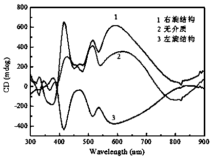
[0066] The circular dichroism of the prepared structure was measured with normal incidence of light, as figure ...
Embodiment 3
[0068] The preparation method of the two-dimensional chiral metal-dielectric nanostructure of this embodiment is the same as that of Embodiment 1, the only difference is that the evaporated metal material is gold, and the insulating material is photoresist. A two-dimensional chiral metal-dielectric nanostructure with a right-handed structure was obtained.
PUM
| Property | Measurement | Unit |
|---|---|---|
| size | aaaaa | aaaaa |
| diameter | aaaaa | aaaaa |
| thickness | aaaaa | aaaaa |
Abstract
Description
Claims
Application Information
 - Generate Ideas
- Intellectual Property
- Life Sciences
- Materials
- Tech Scout
- Unparalleled Data Quality
- Higher Quality Content
- 60% Fewer Hallucinations
Browse by: Latest US Patents, China's latest patents, Technical Efficacy Thesaurus, Application Domain, Technology Topic, Popular Technical Reports.
© 2025 PatSnap. All rights reserved.Legal|Privacy policy|Modern Slavery Act Transparency Statement|Sitemap|About US| Contact US: help@patsnap.com


