Pulse modulation processing circuit
A processing circuit and pulse modulation technology, applied in the field of pulse modulation processing circuits, can solve the problems of non-compliance of output voltage, design requirements and uncontrollable gain, and achieve the effect of realizing linear relationship
- Summary
- Abstract
- Description
- Claims
- Application Information
AI Technical Summary
Problems solved by technology
Method used
Image
Examples
Embodiment 1
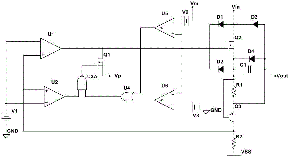
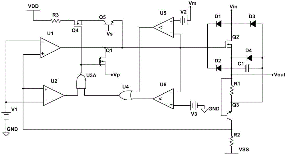
[0022] Such as figure 1 , the reference voltage nodes V1-V4 can be powered by a DC voltage source or a microcontroller voltage output terminal, the overshoot signal is introduced through the input voltage signal Vin, and the working state of the depletion type field effect transistor Q2 is a non-modulation state, That is, the input voltage signal is directly equal to the output voltage signal Vout; for the reference voltage node V2, it is necessary to keep the difference between the input voltage signal and the positive voltage of the reference voltage node V2 higher than the voltage value of the modulation drive signal; when the voltage value of the reference voltage node V3 is higher than Modulate the voltage value of the driving signal or when the comparator U6 outputs a high level, and when an overshoot signal is detected at the non-inverting input terminal of the operational amplifier U2, the NAND gate U3A makes the field effect transistor Q1 cut off, and the operational a...
Embodiment 2
[0025] refer to Figure 4 Describe in detail. Specifically, the charging and discharging circuit 11 includes inverters U8, U9 and U10, a switching transistor Q5, a capacitor C2, a switching transistor Q4 and a power supply VDD. The inverter group receives the initial signal 20 and generates an inverted signal. Each switch triode uses the received inverted signal as a control signal to control the disconnection or conduction between the other two ports, and use it in the PWM circuit 11 . Specifically, when the inverted signal is digital 0, the switch transistor Q5 is turned on, so that the power supply VDD charges the capacitor C2, so that the voltage at the port of the capacitor C2 increases linearly. When the signal is digital 1 after phase inversion, the switching transistor Q5 is turned off, and the switching transistor Q4 is turned on. Therefore, the capacitor C2 is discharged through the switching transistor Q4 , and the voltage at one end of the capacitor C2 connected ...
PUM
 Abstract
Description
Claims
Application Information
 - R&D
- Intellectual Property
- Life Sciences
- Materials
- Tech Scout
- Unparalleled Data Quality
- Higher Quality Content
- 60% Fewer Hallucinations
Browse by: Latest US Patents, China's latest patents, Technical Efficacy Thesaurus, Application Domain, Technology Topic, Popular Technical Reports.
© 2025 PatSnap. All rights reserved.Legal|Privacy policy|Modern Slavery Act Transparency Statement|Sitemap|About US| Contact US: help@patsnap.com


