


Quick Research
Generate reliable direction feasibility study reports for your R&D in just a few steps.

Technical Q&A
Discover and master advanced knowledge NOW. Basics, ideas, possibilities, all at once.

Find Solutions
As an expert in R&D theories, this can generate solutions to your technical problems instantly.

Evaluate Feasibility
Analyze your overall solution with one click, know your potential R&D risks in advance.

Monitor Landscape
Get weekly tech updates, stay abreast of the latest tech innovations and key insights.
High-mobility-ratio lamellar Bi2O2Se semiconductor film and preparation method thereof
A semiconductor and mobility technology, applied in semiconductor devices, coatings, gaseous chemical plating, etc., can solve the problems of single crystal thin film synthesis that have not been reported, difficulties in the field of electronics and optoelectronics, poor crystal quality, etc.
- Summary
- Abstract
- Description
- Claims
- Application Information
AI Technical Summary
Problems solved by technology
Method used
Image

Examples
Embodiment 1
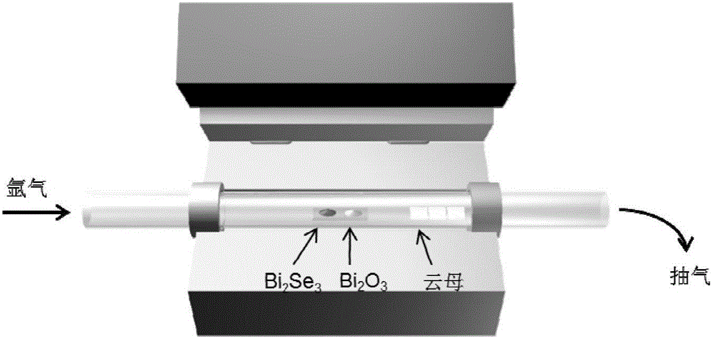
[0032] Weigh 0.71 g Bi 2 o 3 Powder and 1.00 g Bi 2 Se 3 block (molar ratio 1:1), which was placed in the center of the quartz tube of the tube furnace. Next, the fluorophlogopite substrate was placed 10-14 cm downstream from the center of the tube furnace. The carrier gas argon was introduced to maintain the system pressure at 200 Torr. Raise the temperature to 630°C and maintain it for 5 minutes for chemical vapor deposition. After the deposition is completed, the introduction of the carrier gas is stopped, and the temperature is naturally cooled to room temperature, and the deposited Bi 2 o 2 The mica substrate of Se thin film is taken out, promptly obtains the layered Bi provided by the present invention 2 o 2 Se semiconductor film.
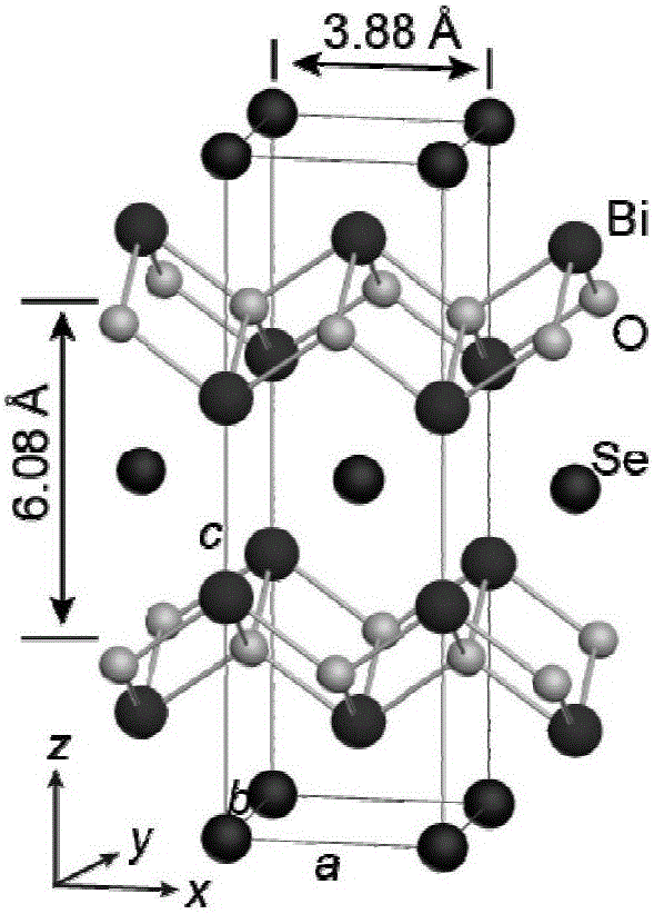
[0033] figure 2 The resulting layered Bi prepared for this example 2 o 2 Crystal structure diagram of Se semiconductor thin film; it can be seen from the figure that Bi 2 o 2 Se is a type composed of (Bi 2 o 2 ) n layer and ...
Embodiment 2
[0040] Weigh 1.42 g Bi 2 o 3 Powder and 1.00 g Bi 2 Se 3 block (molar ratio 2:1), which was placed in the center of the quartz tube of the tube furnace. Subsequently, the fluorophlogopite substrate was placed 10-14 cm downstream from the center of the tube furnace. The carrier gas argon was introduced to maintain the system pressure at 400 Torr. Raise the temperature to 580°C and maintain it for 30 minutes for chemical vapor deposition. After the deposition is completed, the introduction of the carrier gas is stopped, and the temperature is naturally cooled to room temperature, and the deposited Bi 2 o 2 The mica substrate of Se thin film is taken out, obtains the layered Bi that the present invention provides 2 o 2 Se semiconductor film.
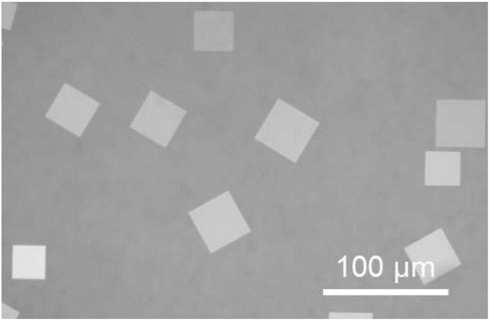
[0041] Figure 8 It is Bi obtained in Example 2 of the present invention 2 o 2 Optical microscope photo of the Se thin film; it can be seen from the figure that the obtained Bi 2 o 2 The domain size of the Se two-dimensional c...
Embodiment 3
[0043] Weigh 2.13 g Bi 2 o 3 Powder and 1.00 g Bi 2 Se 3 block (molar ratio 3:1), which was placed in the center of the quartz tube of the tube furnace. Subsequently, the fluorophlogopite substrate was placed 10-14 cm downstream from the center of the tube furnace. The carrier gas argon was introduced to maintain the system pressure at 50 Torr. Raise the temperature to 680°C and maintain it for 60 minutes for chemical vapor deposition. After the deposition is completed, the introduction of the carrier gas is stopped, and the temperature is naturally cooled to room temperature, and the deposited Bi 2 o 2 The mica substrate of Se thin film is taken out, obtains the layered Bi that the present invention provides 2 o 2 Se semiconductor film.
[0044] Figure 9 Is the obtained Bi of this embodiment 2 o 2 Optical microscope photo of the Se thin film; it can be seen from the figure that the obtained Bi 2 o 2 The Se film is continuous and uniform over a large area.
PUM
| Property | Measurement | Unit |
|---|---|---|
| Size | aaaaa | aaaaa |
| Thickness | aaaaa | aaaaa |
| Hall mobility | aaaaa | aaaaa |
Abstract
Description
Claims
Application Information
 - R&D Engineer
- R&D Manager
- IP Professional
- Industry Leading Data Capabilities
- Powerful AI technology
- Patent DNA Extraction
Browse by: Latest US Patents, China's latest patents, Technical Efficacy Thesaurus, Application Domain, Technology Topic, Popular Technical Reports.
© 2024 PatSnap. All rights reserved.Legal|Privacy policy|Modern Slavery Act Transparency Statement|Sitemap|About US| Contact US: help@patsnap.com