All-medium ultrathin two-dimensional circular polarization dichroic device and preparation method thereof
A two-dimensional circular, all-dielectric technology, applied in the direction of polarizing elements, instruments, optical elements, etc., can solve the problems of small transmittance energy discrimination, low structural discrimination, narrow action band, etc., to achieve low time cost, The effect of wide source of raw materials and easy production
- Summary
- Abstract
- Description
- Claims
- Application Information
AI Technical Summary
Problems solved by technology
Method used
Image
Examples
Embodiment 1
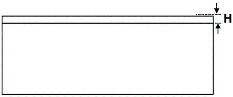
[0030] See attached figure 2 , is a schematic diagram of the front-view structure of the structural unit of an all-dielectric ultra-thin two-dimensional circular polarization dichroic device, wherein the thickness H of silicon in the semiconductor dielectric layer is 0.25 μm; see the attached image 3 , is a top view structure diagram of an all-dielectric ultra-thin two-dimensional circularly polarized dichroic device, in which the longitudinal arm length L1 of the Z-shaped through hole etched in the dielectric layer is 0.2 μm, the transverse arm length L2 is 0.5 μm, and the slit width W is 0.32 μm, and the period P of each structural unit is 0.98 μm.
[0031] attached Figure 4 It is the transmittance curve of left and right circularly polarized light incident through the above-mentioned all-dielectric ultra-thin two-dimensional circularly polarized dichroic device from the silica substrate; attached Figure 5 It is the circular dichroism curve of the all-dielectric ultrat...
Embodiment 2
[0038] In this embodiment, the substrate is silicon dioxide, the semiconductor dielectric layer is silicon; the thickness of the semiconductor dielectric layer is H=0.23 μm, the longitudinal arm length L1 of the Z-shaped through hole is 0.2 μm, and the lateral arm length L2 is 0.5 μm. The width is 0.32 μm, and the period of each structural unit is 0.98 μm. After the semiconductor medium layer is grown by chemical vapor deposition, the circularly polarized polarizer is directly obtained by using a focused ion beam etching process.
[0039] attached Figure 6 It is the transmittance curve of left and right circularly polarized light incident through the above-mentioned all-dielectric ultra-thin two-dimensional circularly polarized dichroic device from the silica substrate; attached Figure 7 It is the circular dichroism curve of the all-dielectric ultrathin two-dimensional circular polarization device. see Figure 6 As shown, there is a large difference in the transmittance o...
Embodiment 3
[0041] The preparation process of this embodiment is consistent with that of Embodiment 1, wherein the substrate is silicon dioxide, and the semiconductor dielectric layer is gallium arsenide; the longitudinal arm length L1 of the Z-shaped through hole is 0.2 μm, and the lateral arm length L2 is 0.5 μm. The slit width is 0.32 μm, and the thickness H of the dielectric layer is 0.25 μm. The period of each structural unit is 0.98 μm.
[0042] attached Figure 8 It is the transmittance curve of left and right circularly polarized light incident through the above-mentioned all-dielectric ultra-thin two-dimensional circularly polarized dichroic device from the silica substrate; attached Figure 9 It is the circular dichroism curve of the all-dielectric ultrathin two-dimensional circular polarization device. see Figure 8 As shown, there is a large difference in the transmittance of the structure to the left and right circularly polarized light in the 1.46μm-1.56μm band. see Fi...
PUM
 Abstract
Description
Claims
Application Information
 - R&D
- Intellectual Property
- Life Sciences
- Materials
- Tech Scout
- Unparalleled Data Quality
- Higher Quality Content
- 60% Fewer Hallucinations
Browse by: Latest US Patents, China's latest patents, Technical Efficacy Thesaurus, Application Domain, Technology Topic, Popular Technical Reports.
© 2025 PatSnap. All rights reserved.Legal|Privacy policy|Modern Slavery Act Transparency Statement|Sitemap|About US| Contact US: help@patsnap.com


