A Transistor Vertical Cavity Surface Emitting Laser

A vertical cavity surface emission and laser technology, which is applied in the direction of semiconductor lasers, lasers, laser components, etc., can solve the problems of restricting device performance and loss of enhanced modulation bandwidth, so as to reduce adverse effects, reduce production costs, and improve lateral distribution. Effect

Active Publication Date: 2019-02-15
苏州长瑞光电有限公司
View PDF8 Cites 0 Cited by
  • Summary
  • Abstract
  • Description
  • Claims
  • Application Information

AI Technical Summary

Problems solved by technology

However, whether it is the T-VCSEL structure proposed by patent SE:2013051451:W or other existing T-VCSEL structures, there is a common key problem that restricts the further improvement of device performance: T-VCSEL increases with the input current, the device The working state of the switch rapidly changes from amplification to saturation, thus losing the function of enhancing the modulation bandwidth

Method used


Image

  • A Transistor Vertical Cavity Surface Emitting Laser
  • A Transistor Vertical Cavity Surface Emitting Laser
  • A Transistor Vertical Cavity Surface Emitting Laser

Examples


Embodiment Construction

[0028] The technical solution of the present invention will be described in detail below in conjunction with the drawings:

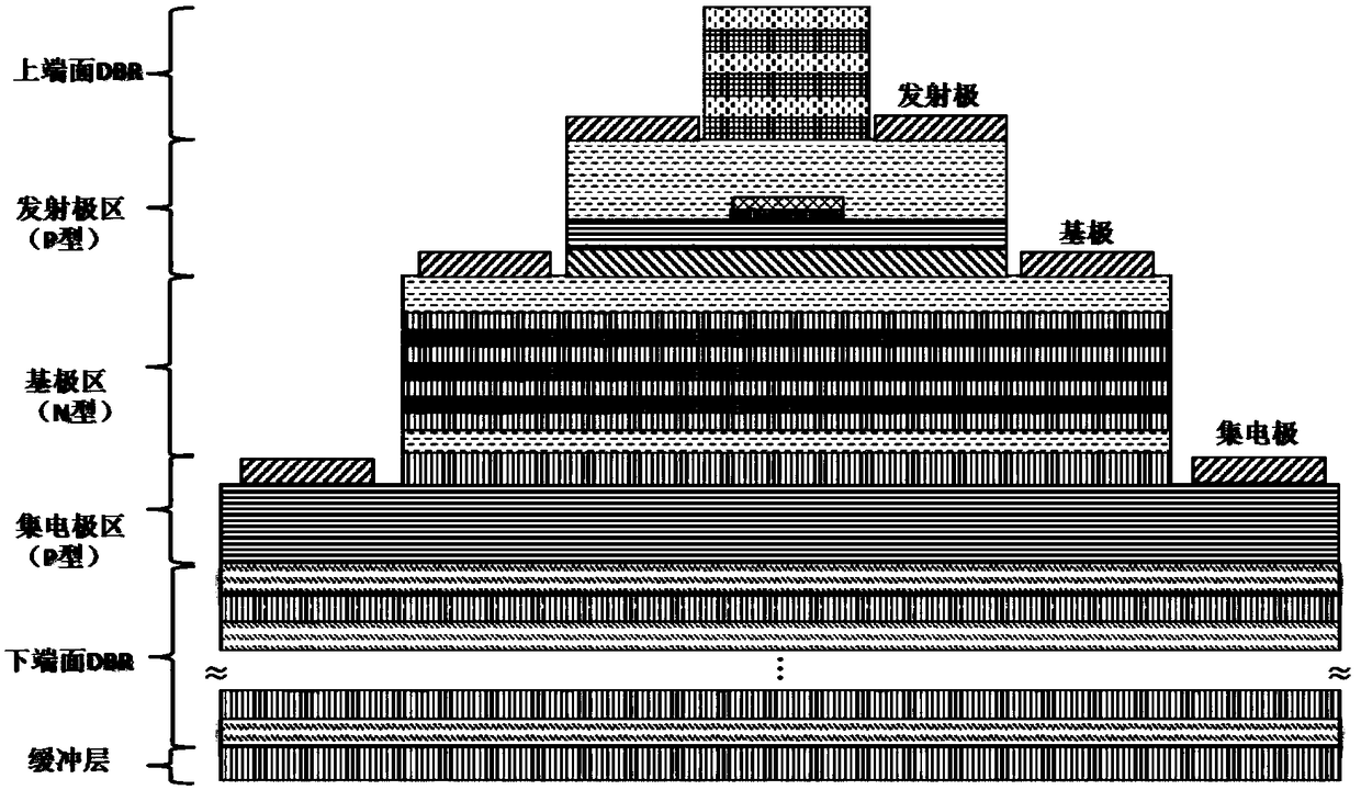
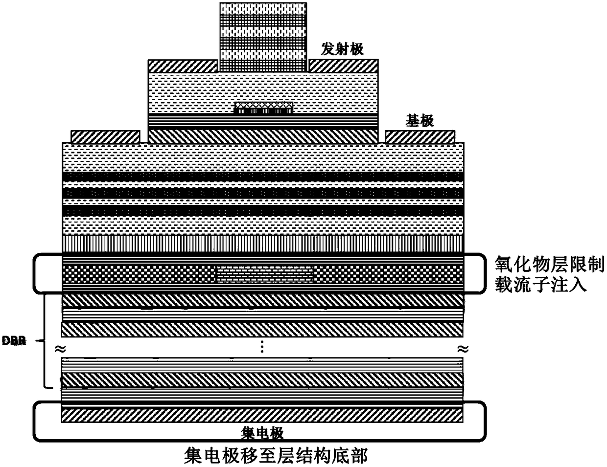
[0029] The existing T-VCSEL has an important defect: as the input current increases, the working state of the device rapidly changes from amplification to saturation, thereby losing the function of enhancing the modulation bandwidth. The essential reason is that due to the limited injection of carriers, stimulated emission mainly occurs in the active area near the center of the device. However, the overall movement path of the carriers includes not only the vertical direction along the center of the device, but also Due to the horizontal direction brought by the position of the corresponding electrode, and the path length of the latter is much longer than the former, this is especially obvious in the collector area. The layer structure of the entire device is only a few microns thick, and the collector is away from the center of the device. The position is ...


PUM


Abstract

The invention discloses a transistor vertical-cavity surface-emitting laser (T-VCSEL), and belongs to the technical field of an integrated photoelectronic device. The T-VCSEL comprises a buffer layer, a lower end face distributed Bragg reflector, a collector region, a base region, an emitter region and an upper end face distributed Bragg reflector which are successively arranged according to an epitaxial growth sequence. The T-VCSEL also comprises a collector, a base electrode and an emitter electrode which are connected with the collector region, the base region and the emitter region. A quantum well active region is arranged in the base region. The collector is arranged on the back of the buffer layer. The buffer layer and the lower end face distributed Bragg reflector are equipped with doping types same as the doping type of the collector region. According to the T-VCSEL, the length of the transmission path of carriers in the collector region is reduced from the existing tens of microns to several microns, and the carriers are imported from the emitter region; therefore, the bad influence of the voltage drop of an internal resistor on the control of the working state of the device can be effectively reduced; and moreover, the transverse distribution of the potential in the collector region is improved.

Description

Technical field [0001] The invention relates to a Transistor Vertical-Cavity Surface-Emitting Laser (T-VCSEL for short), which belongs to the technical field of integrated optoelectronic devices. Background technique [0002] High-speed vertical cavity surface emitting lasers (VCSELs) based on III-V materials have been widely used due to their easy fiber coupling, low threshold current, large direct modulation bandwidth, support for on-chip detection, easy implementation of two-dimensional arrays, and low production costs. Used in short-distance optical communication networks, data centers, and consumer electronic products such as USB, PCI Express, and HDMI. At present, the world's major VCSEL manufacturers have launched products covering 850nm to 1550nm wavelengths and a single channel rate of 25Gb / s. However, with the continuous improvement of bandwidth requirements for short-distance optical communications including on-chip and inter-chip, how to further increase the direct m...

Claims


Application Information

Patent Timeline
Patent Type & Authority Patents(China)
IPC IPC(8): H01S5/183H01S5/187
CPCH01S5/183H01S5/187
Inventor 向宇潘时龙
Owner 苏州长瑞光电有限公司
Why Eureka
Try Eureka