A logic gate circuit based on magnetic field-triggered superlattice phase transition unit
A technology of logic gate circuit and phase change unit, which is applied in the field of logic gate circuit, can solve the problems of high power consumption, complex logic device structure, poor stability, etc., and achieve the effect of superior storage speed and simplified circuit structure
- Summary
- Abstract
- Description
- Claims
- Application Information
AI Technical Summary
Problems solved by technology
Method used
Image

Examples
Embodiment 1
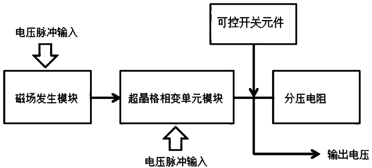
[0059] The logic gate circuit that embodiment 1 provides is as Figure 4 Illustrated: including a superlattice phase change unit 101, a solenoid 107, a controllable switching element 102 and a resistor 103;
[0060] Wherein, the first end of the superlattice phase change unit 101 is used as the first input end 104 of the logic gate circuit, the input end of the solenoid 107 is used as the second input end 106 of the logic gate circuit; End is connected with the second end of superlattice phase change unit 101 and the first end of resistance 103, and its connection point is as the output end 105 of described logic gate circuit; The second end of controllable switch element 102 is grounded, and the second end of resistance 103 The second end is grounded.
[0061] The principle and process of realizing logic functions of the logic gate circuit will be described in detail below in conjunction with the logic gate circuit provided in Embodiment 1.
[0062] When the voltage pulse a...
Embodiment 2
[0075] The logic gate circuit that embodiment 2 provides is as Figure 5 Illustrated: including a superlattice phase change unit 203, a solenoid 207, a controllable switching element 202 and a resistor 201;
[0076] Wherein, the first end of the resistor 201 is used as the first input end 204 of the logic gate circuit, and the input end of the solenoid 207 is used as the second input end 206 of the logic gate circuit; One end is connected, and the other end is connected with the second end of resistance 201; One end of superlattice phase change unit 203 is connected with the second end of resistance 201, and its connection end is as the output end 205 of logic gate circuit, superlattice phase change unit The other end of 203 is grounded.
[0077] The logic gate circuit that embodiment 2 provides can realize logic or OR, and non-NAND, exclusive OR XOR, implication IMP function; The following in conjunction with the logic gate circuit that embodiment 2 provides and Figure 5 ,...
Embodiment 3
[0088] The logic gate circuit that embodiment 3 provides is as Figure 6 Illustrated: including a first superlattice phase change unit 301, a controllable switch element 302, a second superlattice phase change unit 303, a resistor 304, a first solenoid 308 and a second solenoid 309;
[0089] Wherein, the first terminal of the first superlattice phase-change unit 301 is used as the first input terminal 305 of the logic gate circuit, the input terminal of the first solenoid 308 is used as the second input terminal 310 of the logic gate circuit, and the second solenoid The input end of pipe 309 is used as the third input end 311 of logic gate circuit, the first end of the second superlattice phase change unit 303 is used as the fourth input end 306 of logic gate circuit; The second end of the superlattice phase change unit 301 is connected to the second end of the second superlattice phase change unit 303, and the other end of the controllable switch element 302 is grounded; one ...
PUM
 Abstract
Description
Claims
Application Information
 - R&D
- Intellectual Property
- Life Sciences
- Materials
- Tech Scout
- Unparalleled Data Quality
- Higher Quality Content
- 60% Fewer Hallucinations
Browse by: Latest US Patents, China's latest patents, Technical Efficacy Thesaurus, Application Domain, Technology Topic, Popular Technical Reports.
© 2025 PatSnap. All rights reserved.Legal|Privacy policy|Modern Slavery Act Transparency Statement|Sitemap|About US| Contact US: help@patsnap.com