
Anti-jitter circuit, anti-jitter method, and successive approximation analog-to-digital converter based on circuit

A digital-to-analog converter and circuit technology, used in analog-to-digital conversion, code conversion, instruments, etc., can solve problems such as affecting the conversion efficiency of analog-to-digital converters, affecting processing work, and long charging time, and achieving the duration of jitter Short, improve conversion efficiency, improve the effect of precision

Active Publication Date: 2016-08-03
上海锐麟微电子有限公司
View PDF3 Cites 4 Cited by
  • Summary
  • Abstract
  • Description
  • Claims
  • Application Information

AI Technical Summary

Problems solved by technology

[0009] In the traditional DAC converter, the internal capacitor array is charged by the electrical signal transmitted by the bonded wire. From the above analysis, it can be seen that using this original method, on the one hand, makes its output signal V DAC It will send jitter and affect the subsequent processing work; on the one hand, its charging time is longer, which affects the conversion efficiency of the analog-to-digital converter

Method used


Image

  • Anti-jitter circuit, anti-jitter method, and successive approximation analog-to-digital converter based on circuit
  • Anti-jitter circuit, anti-jitter method, and successive approximation analog-to-digital converter based on circuit
  • Anti-jitter circuit, anti-jitter method, and successive approximation analog-to-digital converter based on circuit

Examples


Embodiment Construction

[0055] The technical solutions of the present invention will be described in further detail below with reference to the accompanying drawings, but the protection scope of the present invention is not limited to the following.

[0056] (1) Anti-jitter circuit

[0057] The present invention provides an anti-jitter circuit with high response speed, which is used to reduce the jitter caused by parasitic inductance and parasitic resistance in the integrated circuit and improve the response speed of the integrated circuit.

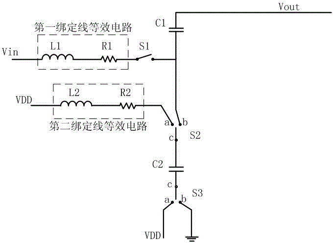
[0058] Such as image 3 As shown, the present invention improves the traditional integrated circuit using the bonding packaging method, which can effectively reduce the jitter caused by the bonding wire, and at the same time, improve the response speed of the integrated circuit.

[0059] The integrated circuit applied in the present invention includes a first parasitic inductance L1, a first parasitic resistance R1, a control switch S1, and a first capacitor C1. The inpu...


PUM


Abstract

The invention discloses an anti-jitter circuit, an anti-jitter method, and a successive approximation analog-to-digital converter based on the circuit. The anti-jitter circuit comprises a parasitic inductor L1, a parasitic inductor L2, a parasitic resistor R1, a parasitic resistor R2, a switch S1, a capacitor C1, a capacitor C2, a switch S2, and a switch S3, wherein the input end of the parasitic inductor L1 is connected with a signal input end Vin, the output end of the parasitic inductor L1 is connected with a signal output end Vout through the parasitic resistor R1, the switch S1 and the capacitor C1 in sequence, the input end of the parasitic inductor L2 is connected with a signal input end VDD, the output end of the parasitic inductor L2 is connected with a fixed port a of the switch S2 through the parasitic resistor R2, a fixed port b of the switch S2 is connected with the signal output end Vout through the capacitor C1, a moving end c of the switch S2 is connected with a moving end c of the switch S3 through the capacitor C2, a fixed port b of the switch S3 is in butt joint with the ground, and a fixed port a of the switch S3 is connected with the signal input end VDD. Jitter caused by binding wires is reduced effectively, and the response speed of the integrated circuit is improved.

Description

Technical field [0001] The present invention relates to the field of integrated circuits, in particular to an anti-jitter circuit with high response speed and its realization method, and a successive approximation analog-to-digital converter designed based on the anti-jitter circuit. Background technique [0002] The main parasitic elements generated by printed circuit board wiring include: parasitic resistance, parasitic capacitance and parasitic inductance. For example: the parasitic resistance of the PCB is formed by the traces between the components; the traces, pads and flat traces on the circuit board will generate parasitic capacitance; the parasitic inductance is generated by loop inductance, mutual inductance and vias. When converting the circuit schematic into an actual PCB, all these parasitic components may interfere with the effectiveness of the circuit. [0003] Generally, IC chips are packaged by bonding packaging. Products made by bonding packaging have the advanta...

Claims


Application Information

Patent Timeline
Patent Type & Authority Applications(China)
IPC IPC(8): H03M1/38
Inventor 李彪向建军何天长叶飞
Owner 上海锐麟微电子有限公司
Learn More