A kind of blue light-emitting silicon oxide nanomaterial and its preparation method
A technology of nanomaterials and silicon oxide, applied in the direction of luminescent materials, chemical instruments and methods, etc., can solve the problems of harsh preparation conditions, complicated steps, and few reports on the optical properties of silicon oxide nanomaterials, and achieve strong blue light emission characteristics, methods Simple, easily sized effects
- Summary
- Abstract
- Description
- Claims
- Application Information
AI Technical Summary
Problems solved by technology
Method used
Image
Examples
Embodiment 1
[0025] Example 1. On Si / SiO 2 The preparation of silicon oxide nanomaterials includes the following basic steps:
[0026] (1) on Si / SiO 2 Ti films with a thickness of 5nm were prepared on the surface to form Si / SiO 2 / Ti structure;
[0027] (2) Si / SiO 2 / Ti is placed in the reaction chamber, and the reaction chamber is evacuated;
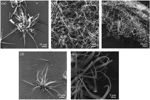
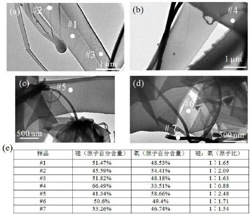
[0028] (3) Inject H into the reaction chamber 2 S gas, processing Si / SiO at 450°C 2 / Ti for about 20 minutes, and then lower the temperature to obtain silicon oxide nanomaterials. The scanning electron microscope image of the as-prepared silicon oxide nanobelts is shown in figure 1 (a) and transmission electron microscopy image 3 (a) shown.
Embodiment 2
[0029] Example 2. On Si / SiO 2 Preparation of silica nanomaterials on:
[0030] Similar to the steps in Example 1, the metal Ti film can be replaced with other metals, such as Cr, Cu, Mo, Ru, Pt, Ni, Pd, Au, Al or Fe, and the thickness of the metal film is in the range of 0.5nm to 50nm Silicon oxide nanomaterials can be obtained both internally and at a treatment temperature of 450°C to 1030°C. like figure 1 (b) is for Si / SiO 2 / Cr (25nm) was subjected to a heat treatment at 950°C for 40 minutes to obtain a scanning electron microscope image of a silicon oxide nanomaterial.
Embodiment 3
[0031] Embodiment 3. prepare silicon oxide nanomaterial on glass, comprise the following basic steps:
[0032] (1) preparing an Au film with a thickness of 10 nm on the glass to form a glass / Au structure;
[0033] (2) Place the glass / Au in the reaction chamber and evacuate the reaction chamber;
[0034] (3) Inject H into the reaction chamber 2 S gas, treat S glass / Au at 700°C for about 80 minutes, and then lower the temperature to obtain silicon oxide nanomaterials. The scanning electron microscope image of the as-prepared silicon oxide nanobelts is shown in figure 1 (c) and transmission electron microscopy image 3 (b) shown.
[0035] Similarly, the metal Au film can be replaced with other metals, such as Ti, Cr, Cu, Mo, Ru, Pt, Ni, Pd, Al or Fe, the thickness of the metal film is in the range of 0.5nm to 50nm, and the treatment temperature is 450 ℃ ~ 1030 ℃ can be obtained silicon oxide nanomaterials.
[0036] Similarly, glass can be replaced with quartz. The scanning...
PUM
| Property | Measurement | Unit |
|---|---|---|
| thickness | aaaaa | aaaaa |
Abstract
Description
Claims
Application Information
 - R&D
- Intellectual Property
- Life Sciences
- Materials
- Tech Scout
- Unparalleled Data Quality
- Higher Quality Content
- 60% Fewer Hallucinations
Browse by: Latest US Patents, China's latest patents, Technical Efficacy Thesaurus, Application Domain, Technology Topic, Popular Technical Reports.
© 2025 PatSnap. All rights reserved.Legal|Privacy policy|Modern Slavery Act Transparency Statement|Sitemap|About US| Contact US: help@patsnap.com


