Filter coating and lamp filtering device
A technology of a filter device and a filter film, which is applied to lighting devices, independent lighting devices, components of lighting devices, etc., to achieve the effects of a simple manufacturing method, reducing light transmission, and avoiding direct exposure of excessively strong light.
- Summary
- Abstract
- Description
- Claims
- Application Information
AI Technical Summary
Problems solved by technology
Method used
Image
Examples
Embodiment 1
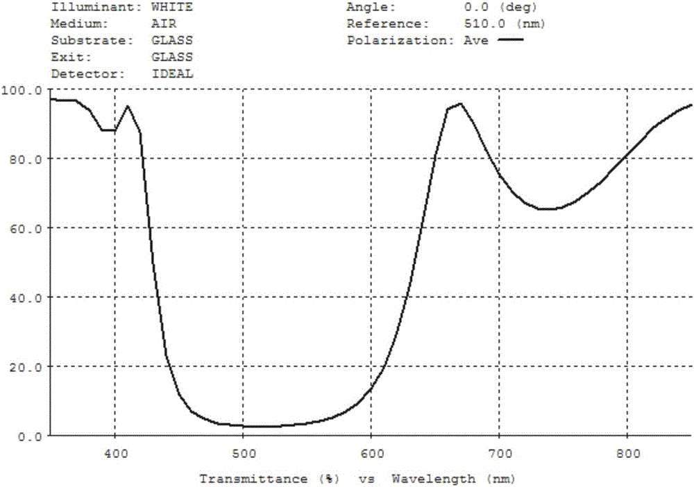
[0032] The filter film is formed by alternately stacking titanium dioxide layers 1 formed by depositing titanium dioxide by vacuum evaporation or sputtering and silicon dioxide layers 2 formed by depositing silicon dioxide by vacuum evaporation or sputtering. The titanium dioxide layers 1 and The silicon dioxide layer 2 has a total of 10 layers, the first layer is titanium dioxide layer 1, the second layer is silicon dioxide layer 2, the third layer is titanium dioxide layer 1, the fourth layer is silicon dioxide layer 2, and the fifth layer is titanium dioxide Layer 1, the sixth layer is silicon dioxide layer 2, the seventh layer is titanium dioxide layer 1, the eighth layer is silicon dioxide layer 2, the ninth layer is titanium dioxide layer 1, and the tenth layer is silicon dioxide layer 2, each The optical thickness of the layers is 118nm-133nm, and the optical thickness of each layer is different. The spectral transmission curve of this kind of filter film that transmits...
Embodiment 2
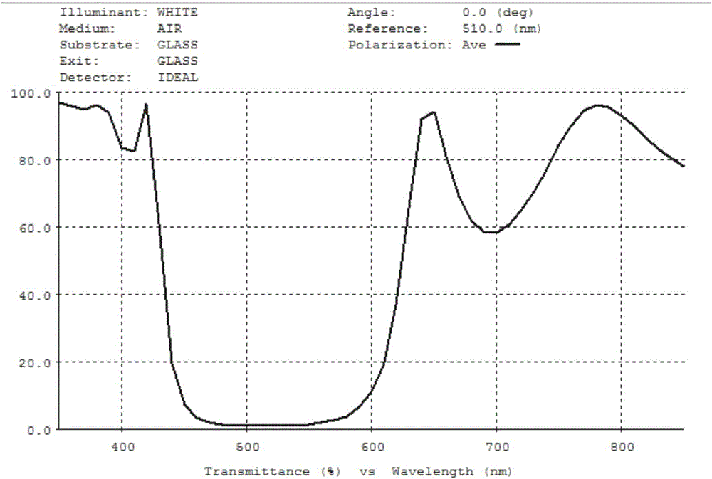
[0034] The filter film is formed by alternately stacking titanium dioxide layers 1 formed by depositing titanium dioxide by vacuum evaporation or sputtering and silicon dioxide layers 2 formed by depositing silicon dioxide by vacuum evaporation or sputtering. The titanium dioxide layers 1 and The silicon dioxide layer 2 has a total of 12 layers, the first layer is titanium dioxide layer 1, the second layer is silicon dioxide layer 2, the third layer is titanium dioxide layer 1, the fourth layer is silicon dioxide layer 2, and the fifth layer is titanium dioxide Layer 1, the sixth layer is silicon dioxide layer 2, the seventh layer is titanium dioxide layer 1, the eighth layer is silicon dioxide layer 2, the ninth layer is titanium dioxide layer 1, the tenth layer is silicon dioxide layer 2, the The eleventh layer is a titanium dioxide layer 1 , and the twelfth layer is a silicon dioxide layer 2 . The optical thickness of each layer is 118nm-133nm, and the optical thickness of ...
Embodiment 3
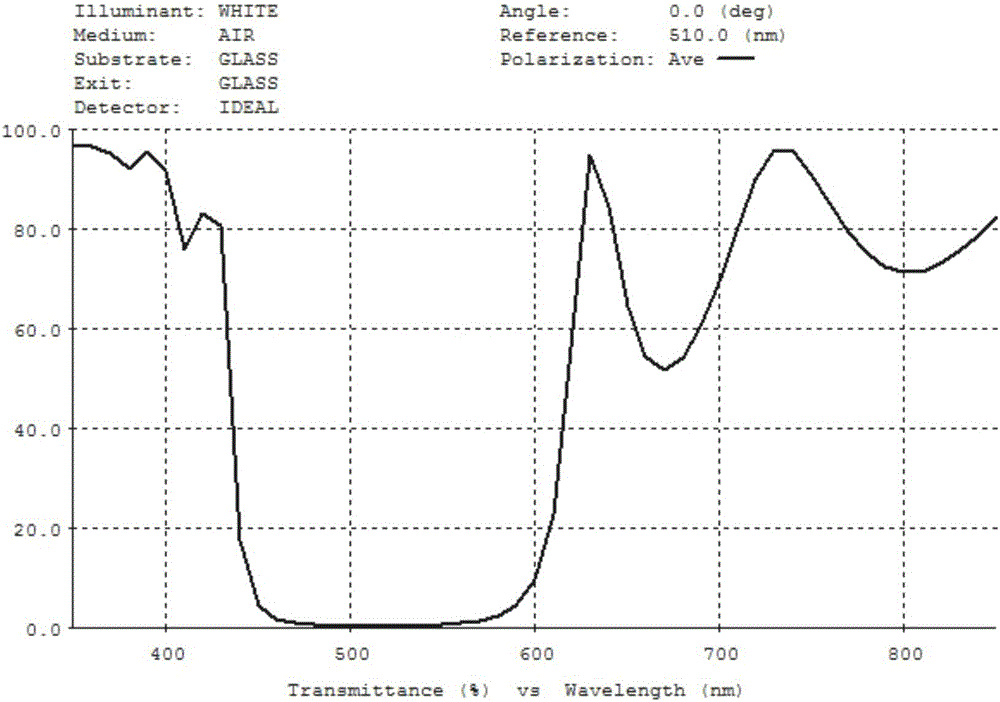
[0036] The filter film is formed by alternately stacking titanium dioxide layers 1 formed by depositing titanium dioxide by vacuum evaporation or sputtering and silicon dioxide layers 2 formed by depositing silicon dioxide by vacuum evaporation or sputtering. The titanium dioxide layers 1 and Silicon dioxide layer 2 has a total of 14 layers, the first layer is titanium dioxide layer 1, the second layer is silicon dioxide layer 2, the third layer is titanium dioxide layer 1, the fourth layer is silicon dioxide layer 2, and the fifth layer is titanium dioxide Layer 1, the sixth layer is silicon dioxide layer 2, the seventh layer is titanium dioxide layer 1, the eighth layer is silicon dioxide layer 2, the ninth layer is titanium dioxide layer 1, the tenth layer is silicon dioxide layer 2, the The eleventh layer is a titanium dioxide layer 1 , the twelfth layer is a silicon dioxide layer 2 , the thirteenth layer is a titanium dioxide layer 1 , and the fourteenth layer is a silicon...
PUM
 Abstract
Description
Claims
Application Information
 - R&D
- Intellectual Property
- Life Sciences
- Materials
- Tech Scout
- Unparalleled Data Quality
- Higher Quality Content
- 60% Fewer Hallucinations
Browse by: Latest US Patents, China's latest patents, Technical Efficacy Thesaurus, Application Domain, Technology Topic, Popular Technical Reports.
© 2025 PatSnap. All rights reserved.Legal|Privacy policy|Modern Slavery Act Transparency Statement|Sitemap|About US| Contact US: help@patsnap.com


