Method for preparing Fresnel lens on sapphire window and its application
A Fresnel lens and sapphire technology, which is applied in the field of optical components, can solve the problems such as the reduction of the detection range of ultraviolet detectors and the influence of sensitivity, and achieve the effect of large optical filling factor.
- Summary
- Abstract
- Description
- Claims
- Application Information
AI Technical Summary
Problems solved by technology
Method used
Image
Examples
Embodiment 1
[0025] This embodiment includes the following steps:
[0026] In the first step, according to the chip size of the ultraviolet detector, determine the size and focal length of the Fresnel lens, design the layout and determine the etching depth.
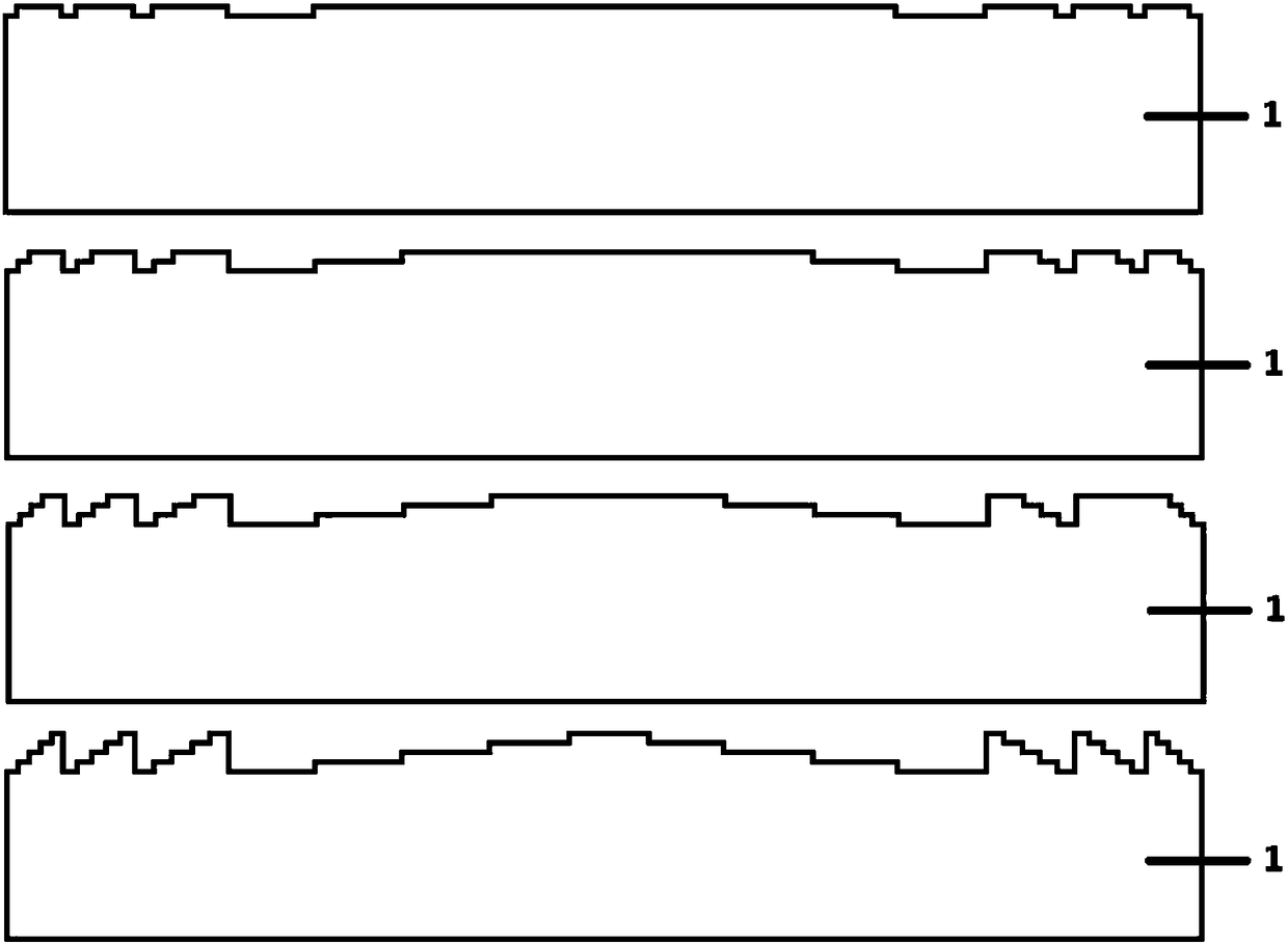
[0027] The second step is to etch a specific pattern on the silicon wafer by using reactive ion etching Si micromachining technology. The four etching depths are equal, each etching is 280nm, and the total step height is 1.12μm, so that UV protection can be achieved. focus function.
[0028] In the third step, an imprint template is prepared from the above-mentioned silicon wafer with the Fresnel lens structure.
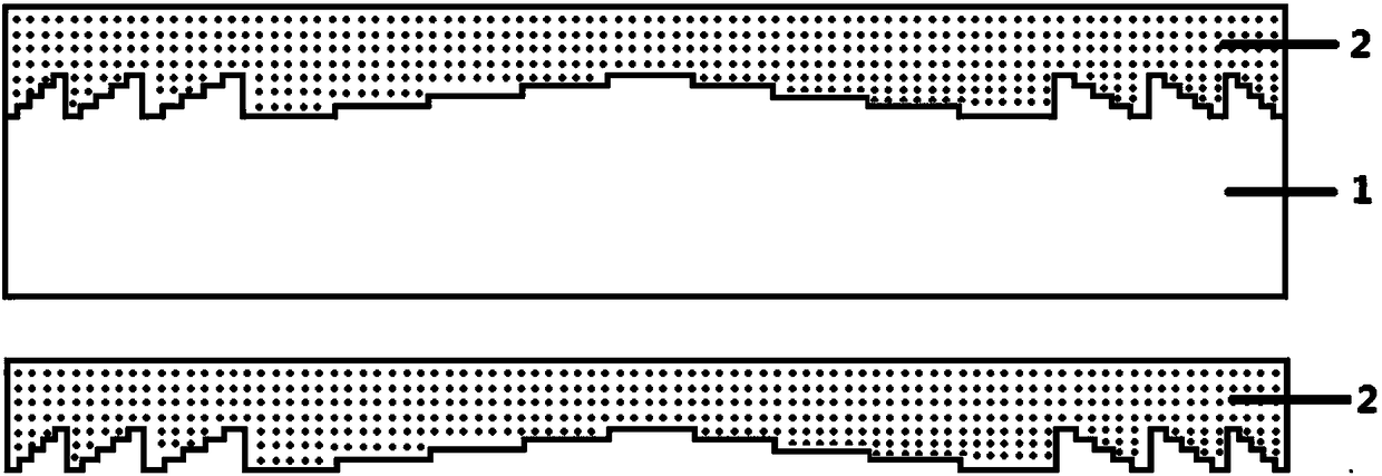
[0029] In the fourth step, after the photoresist is spin-coated on the sapphire window, the above-mentioned imprint template is used for imprinting, and then an etching process is performed to form a sapphire window with a Fresnel lens structure.
[0030] The ultraviolet detectors include but are not limited to: GaN, SiC, ...
Embodiment 2
[0037] This embodiment includes the following steps:
[0038] In the first step, according to the chip size of the ultraviolet detector, determine the size and focal length of the Fresnel lens, design the layout and determine the etching depth.
[0039] In the second step, a specific pattern is etched on the silicon wafer using reactive ion etching Si micromachining technology. focus function.
[0040] In the third step, an imprint template is prepared from the above-mentioned silicon wafer with the Fresnel lens structure.
[0041] In the fourth step, after the photoresist is spin-coated on the sapphire window, the above-mentioned imprint template is used for imprinting, and then an etching process is performed to form a sapphire window with a Fresnel lens structure.
[0042] The ultraviolet detectors include but are not limited to: GaN, SiC, Al x Ga 1-x N, CdS, ZnO, diamond and other UV detectors.
[0043] In the four-layer mask nested dry etching process for silicon waf...
Embodiment 3
[0049] This embodiment includes the following steps:
[0050] In the first step, according to the chip size of the ultraviolet detector, determine the size and focal length of the Fresnel lens, design the layout and determine the etching depth.
[0051] In the second step, a specific pattern is etched on the silicon wafer using the reactive ion etching Si micromachining process. The depth of the four etchings is equal, each etching is 400nm, and the total step height is 1.6μm, so that the UV radiation can be realized. focus function.
[0052] In the third step, an imprint template is prepared from the above-mentioned silicon wafer with the Fresnel lens structure.
[0053] In the fourth step, after the photoresist is spin-coated on the sapphire window, the above-mentioned imprint template is used for imprinting, and then an etching process is performed to form a sapphire window with a Fresnel lens structure.
[0054] The ultraviolet detectors include but are not limited to: G...
PUM
 Abstract
Description
Claims
Application Information
 - R&D
- Intellectual Property
- Life Sciences
- Materials
- Tech Scout
- Unparalleled Data Quality
- Higher Quality Content
- 60% Fewer Hallucinations
Browse by: Latest US Patents, China's latest patents, Technical Efficacy Thesaurus, Application Domain, Technology Topic, Popular Technical Reports.
© 2025 PatSnap. All rights reserved.Legal|Privacy policy|Modern Slavery Act Transparency Statement|Sitemap|About US| Contact US: help@patsnap.com


