High-performance pore filling and copper plating solution
A solution and copper plating technology, which is applied to the formation of electrical connection of printed components, electrical components, printed circuit manufacturing, etc., can solve the problems of narrow copper plating solution process window, high organic carbon content, easy aging and failure, etc., to achieve outstanding substantive Features, life extension, effect of improving plating quality
- Summary
- Abstract
- Description
- Claims
- Application Information
AI Technical Summary
Problems solved by technology
Method used
Image
Examples
Embodiment 1
[0023] The additive prepared by the present invention is added to the copper plating basic solution, the mass fraction of the additive in the basic solution is 1 ppm, and the copper plating basic solution is a combination of copper methanesulfonate and methanesulfonic acid, wherein , The concentration of copper methanesulfonate is 250g / L, and the concentration of methanesulfonic acid is 40g / L.
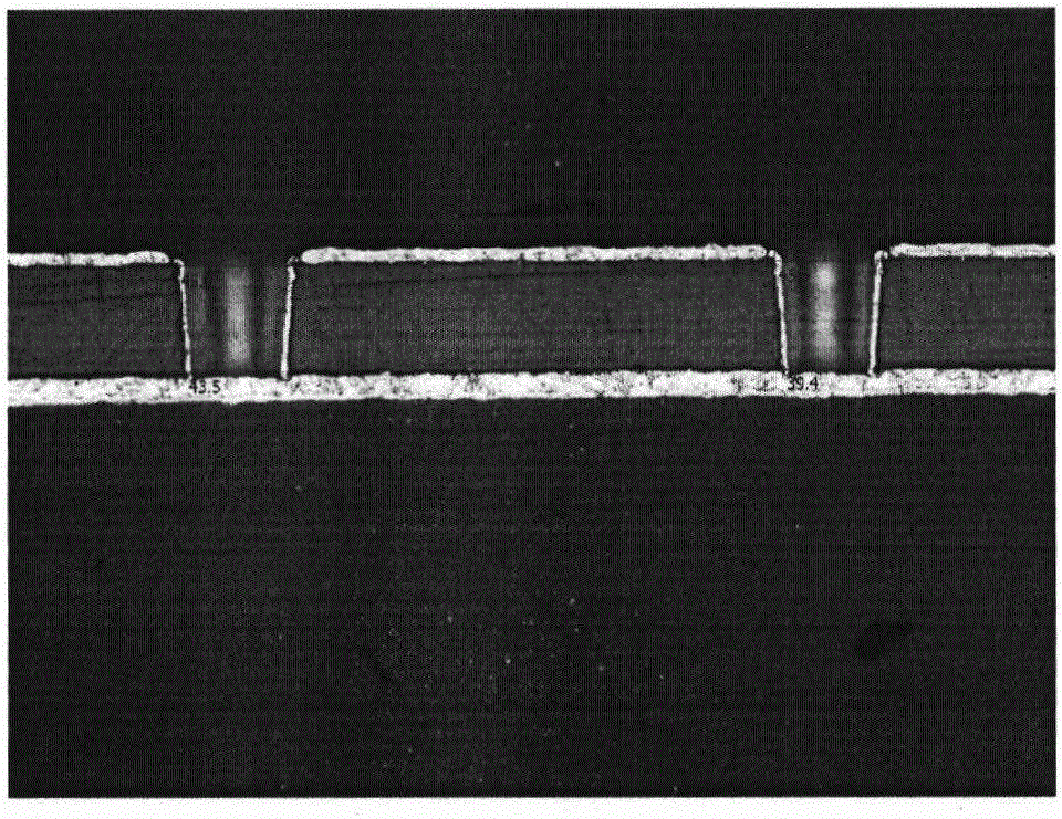
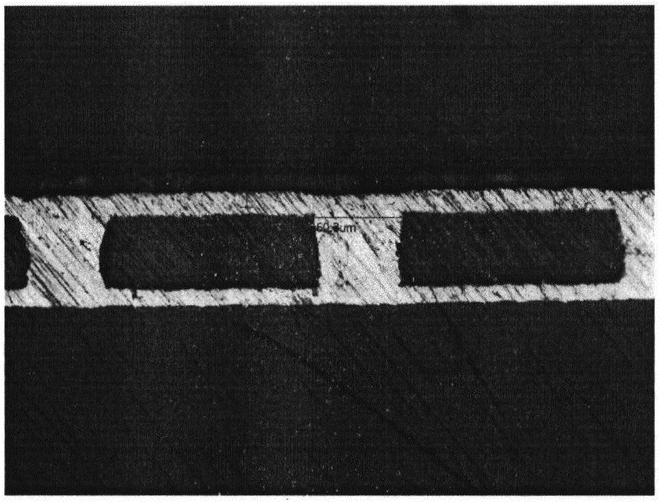
[0024] Using the copper plating solution prepared above, the cleaned hole-filled samples were plated with hole-filling under the conditions of a current density of 1.5ASD and a plating time of 40min. The effective filling aperture is 60-80μm and the thickness-to-diameter ratio is 0.5- For blind holes of 1, the surface copper thickness is controlled below 10μm. The metallographic microscope pictures of the sample before and after the hole filling and electroplating are as follows: figure 1 with figure 2 .
Embodiment 2
[0026] The additive prepared by the present invention is added to the copper plating basic solution, the mass fraction of the additive in the basic solution is 0.8 ppm, and the copper plating basic solution is composed of a combination of copper methanesulfonate and methanesulfonic acid, Among them, the concentration of copper methanesulfonate is 300 g / L, and the concentration of methanesulfonic acid is 60 g / L.
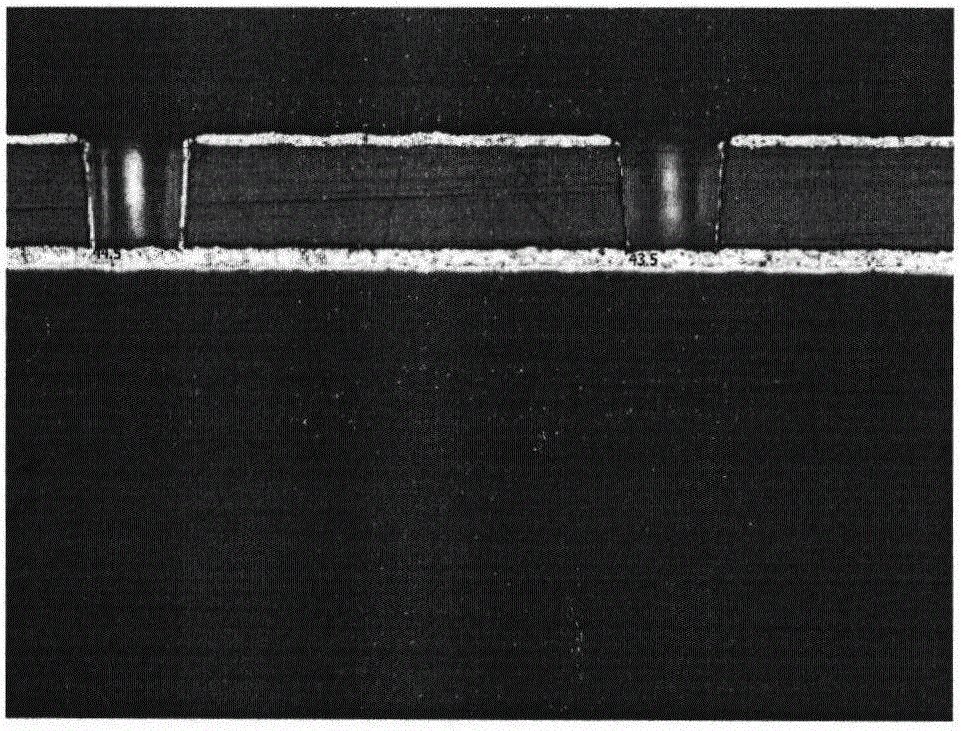
[0027] The cleaned hole-filled sample is electroplated under the conditions of current density of 1.6ASD and plating time of 35min. The effective filling of blind holes with a diameter of 50-60μm and a thickness-to-diameter ratio of 0.5-1, the copper thickness of the surface is controlled within 10μm or less. The metallographic microscope pictures of the sample before and after the hole filling and electroplating are as follows: image 3 with Figure 4 .
PUM
| Property | Measurement | Unit |
|---|---|---|
| concentration | aaaaa | aaaaa |
| concentration | aaaaa | aaaaa |
Abstract
Description
Claims
Application Information
 - R&D
- Intellectual Property
- Life Sciences
- Materials
- Tech Scout
- Unparalleled Data Quality
- Higher Quality Content
- 60% Fewer Hallucinations
Browse by: Latest US Patents, China's latest patents, Technical Efficacy Thesaurus, Application Domain, Technology Topic, Popular Technical Reports.
© 2025 PatSnap. All rights reserved.Legal|Privacy policy|Modern Slavery Act Transparency Statement|Sitemap|About US| Contact US: help@patsnap.com


