


Quick Research
Generate reliable direction feasibility study reports for your R&D in just a few steps.

Technical Q&A
Discover and master advanced knowledge NOW. Basics, ideas, possibilities, all at once.

Find Solutions
As an expert in R&D theories, this can generate solutions to your technical problems instantly.

Evaluate Feasibility
Analyze your overall solution with one click, know your potential R&D risks in advance.

Monitor Landscape
Get weekly tech updates, stay abreast of the latest tech innovations and key insights.
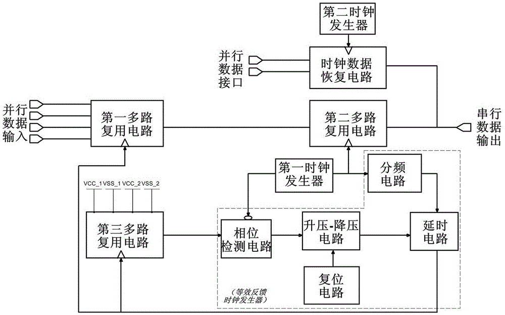
Buffer serial circuit based on transient voltage suppression
An instantaneous voltage suppression and circuit technology, applied in the field of signal conversion, can solve the problems of slow data serial speed, switching loss, mismatch of acquisition clock frequency, etc., achieve the reduction of rising edge time and falling edge time, reduce system loss and waveform Jitter, the effect of improving energy utilization
- Summary
- Abstract
- Description
- Claims
- Application Information
AI Technical Summary
Problems solved by technology
Method used
Image


Examples
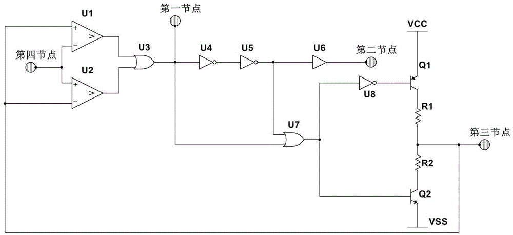
Embodiment 1
[0022] figure 2 For the embodiment of the reset circuit of the present invention, the inverter U4 and the inverter U5 are the simplest delay devices in this embodiment, and the delay circuit can be used to replace the inverter U4 and the inverter U5 to obtain better Initialize function. After replacement, the fourth node is a reference voltage input node, and its size depends on the selected comparator and the threshold voltage that the comparator needs to set. The OR gate U3 is based on the second comparison signal output by the comparator U1 and the comparator U2, the second Three comparison signals to generate a first control signal, and the first control signal output by the OR gate U3 is sent to the first node. The delay circuit delays the first control signal, and the delay interval depends on the reference voltage input from the fourth node. Specifically, the delay time depends on the magnitude of the reference voltage difference input from the fourth node and the loa...
Embodiment 2
[0024] image 3 For the embodiment of the delay circuit of the present invention, the buffers U9-U12 connected in series are connected to the adjustable capacitors C1-C3 in stages; the fifth node and the seventh node are input nodes, and the sixth node is an output node; the seventh The node is connected to a boost-buck circuit, the boost-buck circuit controls the capacitance of the adjustable capacitor, and the buffers U9-U12 generate a phase delay.
Embodiment 3
[0026]The step-up-step-down circuit, that is, the BOOST circuit, can be reduced and replaced according to the actual space occupied by the circuit; for example, when a smaller circuit space is required, it can be replaced with a charge pump. Charge pump, its energy storage device can be a capacitor, the output terminal is the collector and emitter of multiple channel complementary transistors connected in series and symmetrical about the output terminal, the input terminal is the base of multiple transistors, and the logic implemented according to the needs A certain logic gate is added to the base to realize the charge pump; compared with the BOOST circuit, the layout of the charge pump is relatively small, the circuit structure does not require an inductor, and the response speed is extremely fast.
PUM
 Abstract
Description
Claims
Application Information
 - R&D Engineer
- R&D Manager
- IP Professional
- Industry Leading Data Capabilities
- Powerful AI technology
- Patent DNA Extraction
Browse by: Latest US Patents, China's latest patents, Technical Efficacy Thesaurus, Application Domain, Technology Topic, Popular Technical Reports.
© 2024 PatSnap. All rights reserved.Legal|Privacy policy|Modern Slavery Act Transparency Statement|Sitemap|About US| Contact US: help@patsnap.com