Absorption-type optical modulator structure based on ITO material
An optical modulator and absorption type technology, applied in the field of optoelectronics, to achieve the effects of reducing device size, simple waveguide structure design, and simple manufacturing process
- Summary
- Abstract
- Description
- Claims
- Application Information
AI Technical Summary
Problems solved by technology
Method used
Image
Examples
Embodiment
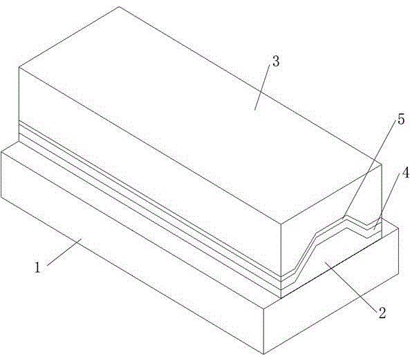
[0032] The schematic diagram of the three-dimensional structure of the absorbing optical modulator based on the ITO material in this embodiment is as follows figure 1 As shown; the light wave with a wavelength of 1.55 μm is used, the first optical waveguide layer, the first optical waveguide layer has a trapezoidal structure, the ITO layer, HfO 2 The isolation layer and the second optical waveguide layer sequentially cover the first optical waveguide layer. The material of the base layer is SiO 2 , the materials of the first optical waveguide layer and the second optical waveguide layer are both Si, the length of the lower base of the trapezoidal structure of the first optical waveguide layer is 0.3 μm, the length of the upper base is 0.2 μm, and the height is 0.17 μm; The surface has a rectangular structure with a height of 0.17 μm and a width of 0.3 μm, HfO 2 The thickness of the isolation layer was 5 nm.
[0033] figure 1 It is a schematic diagram of a three-dimensional...
PUM
| Property | Measurement | Unit |
|---|---|---|
| thickness | aaaaa | aaaaa |
| thickness | aaaaa | aaaaa |
| length | aaaaa | aaaaa |
Abstract
Description
Claims
Application Information
 - R&D
- Intellectual Property
- Life Sciences
- Materials
- Tech Scout
- Unparalleled Data Quality
- Higher Quality Content
- 60% Fewer Hallucinations
Browse by: Latest US Patents, China's latest patents, Technical Efficacy Thesaurus, Application Domain, Technology Topic, Popular Technical Reports.
© 2025 PatSnap. All rights reserved.Legal|Privacy policy|Modern Slavery Act Transparency Statement|Sitemap|About US| Contact US: help@patsnap.com


