
Multi-spectral phase-type metasurface device

A metasurface and phase-type technology, applied in the field of metamaterials, can solve problems such as complex optical systems, and achieve the effect of simple and compact structure, favorable processing and light weight

Active Publication Date: 2016-06-15
INST OF OPTICS & ELECTRONICS - CHINESE ACAD OF SCI
View PDF9 Cites 33 Cited by
  • Summary
  • Abstract
  • Description
  • Claims
  • Application Information

AI Technical Summary

Problems solved by technology

However, the optical system of the traditional STED fluorescence scanning microscope is very complicated, and there is an urgent need to use a single optical element to generate two required spots.
However, in STED microscopy systems, the focal length of traditional metasurface lenses is wavelength-dependent, which has an adverse effect on multispectral imaging.

Method used


Image

  • Multi-spectral phase-type metasurface device
  • Multi-spectral phase-type metasurface device
  • Multi-spectral phase-type metasurface device

Examples


Embodiment 1

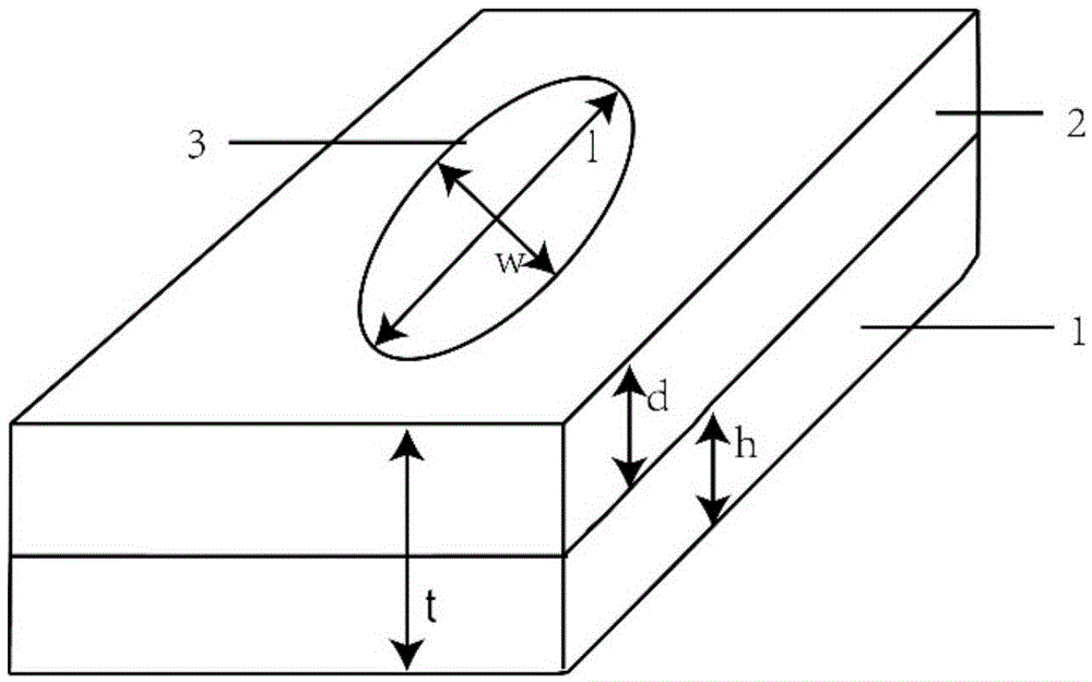
[0037] Example 1 of the present invention takes the preferred elliptical nanopore unit structure as an example, such as figure 1 As shown, the multi-spectral phase-type metasurface device includes a substrate 1, a metasurface layer 2, and a nanopore 3 etched in the metasurface layer that are sequentially arranged from bottom to top. The thickness of the substrate is h; the thickness of the metasurface layer is d; the total thickness of the material is t; the characteristic dimension w (short axis) and l (long axis) of the nanopore structure are not equal. According to this structure, its design principle will be explained in detail below.

[0038] Under CPL incidence of circularly polarized light, each nanohole acts as a polarizing filter, so the spatially varying hole array produces spatially varying polarization states. Due to photon spin-orbit interactions, polarization state changes are related to phase changes. The transmitted light produces a phase delay of 2σα, where ...

Embodiment 2

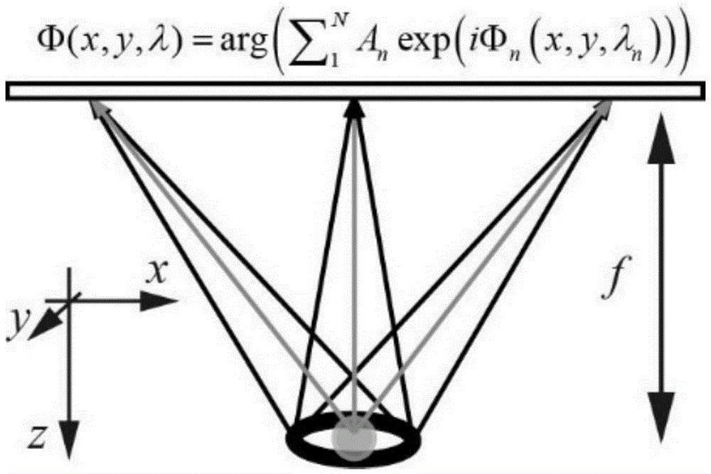
[0055] Focusing and imaging of different wavelengths at the same location are achieved by using multispectral phase-type metasurface devices. According to the above design theory, it is assumed that there are several point light sources with different wavelengths at the same position, and their phase distributions on the metasurface can be expressed as:

[0056] Φ ( x , y ) = arg ( Σ 1 N E n ) = arg ( Σ 1 N A exp ( i 2 π λ n ...

Embodiment 3

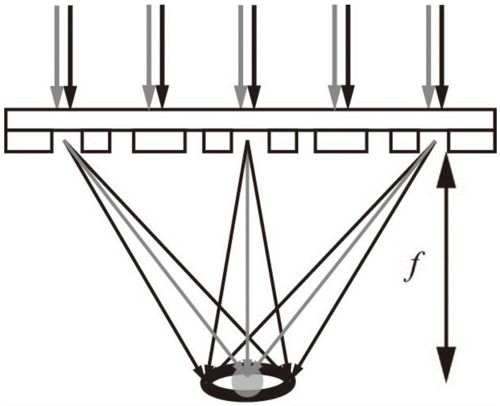
[0060] The multispectral phase-type metasurface device is used to realize the focusing of light waves with different wavelengths and different angles at the same position. Different from Embodiment 2, in this embodiment, light waves incident at different angles are used to focus at the same position, and the phase distribution of the corresponding metasurface can be expressed as:

[0061] Φ ( x , y ) = arg ( Σ 1 N A exp ( i 2 π λ n x 2 + y 2 ...


PUM


Abstract

The invention discloses a multi-spectral phase-type metasurface device and belongs to the metamaterial technical field. The multi-spectral phase-type metasurface device of the invention is composed of a nano unit structure array which is formed on ultra-thin metal or a medium through etching. According to the multi-spectral phase-type metasurface device of the invention, multi-frequency information is coded onto a metasurface; and phase regulation can be performed on electromagnetic waves of a plurality of wavelengths by using wide-band spin-orbit interaction of nanostructures on the metasurface, so that the electromagnetic waves with different wavelengths and different incident angles can be focused to a specific shape. Therefore, the multi-spectral phase-type metasurface device of the invention can be applied to the design of a multi-wavelength ultra-small optical device and an integrated optical system.

Description

technical field [0001] The invention relates to the technical field of metamaterials, in particular to a multispectral phase type metasurface device. Background technique [0002] In modern electromagnetics, the independent control of electromagnetic waves in different frequency bands is very important in applications such as wireless communication and multispectral imaging. However, the existence of material dispersion limits the development of conventional technologies, making corresponding devices and systems bulky, bulky, and limited in performance. [0003] As two-dimensional metamaterials, metasurfaces have been demonstrated to achieve comprehensive modulation of the amplitude, phase, and polarization state of electromagnetic waves, and the wavefront can be arbitrarily modulated using the laws of reflection and refraction in the case of metasurfaces. Thus many functions such as beam steering, focusing and imaging are possible. Because metasurfaces are thinner and eas...

Claims


Application Information

Patent Timeline
IPC IPC(8): G02B1/00G02B5/00
CPCG02B1/002G02B5/00
Inventor 罗先刚赵泽宇王彦钦李雄马晓亮蒲明博
Owner INST OF OPTICS & ELECTRONICS - CHINESE ACAD OF SCI
Learn More