A layout structure of well-isolated anti-SEU multi-node flipping memory cells

A technology of memory cell and layout structure, applied in the direction of electrical components, semiconductor devices, transistors, etc., can solve the problems of ordinary DICE memory cell inversion, etc., to improve the anti-SEU performance, solve poor reliability, and reduce the probability of multi-node inversion. Effect

Active Publication Date: 2018-11-06
BEIJING MXTRONICS CORP +1
View PDF4 Cites 0 Cited by
  • Summary
  • Abstract
  • Description
  • Claims
  • Application Information

AI Technical Summary

Problems solved by technology

[0005] The technical problem solved by the present invention is to overcome the problem that common DICE storage units in the ultra-deep sub-micron process will cause multiple storage nodes in the unit to flip under the influence of SEU, and eventually lead to the flipping of common DICE storage cells

Method used


Image

  • A layout structure of well-isolated anti-SEU multi-node flipping memory cells
  • A layout structure of well-isolated anti-SEU multi-node flipping memory cells
  • A layout structure of well-isolated anti-SEU multi-node flipping memory cells

Examples


Embodiment Construction

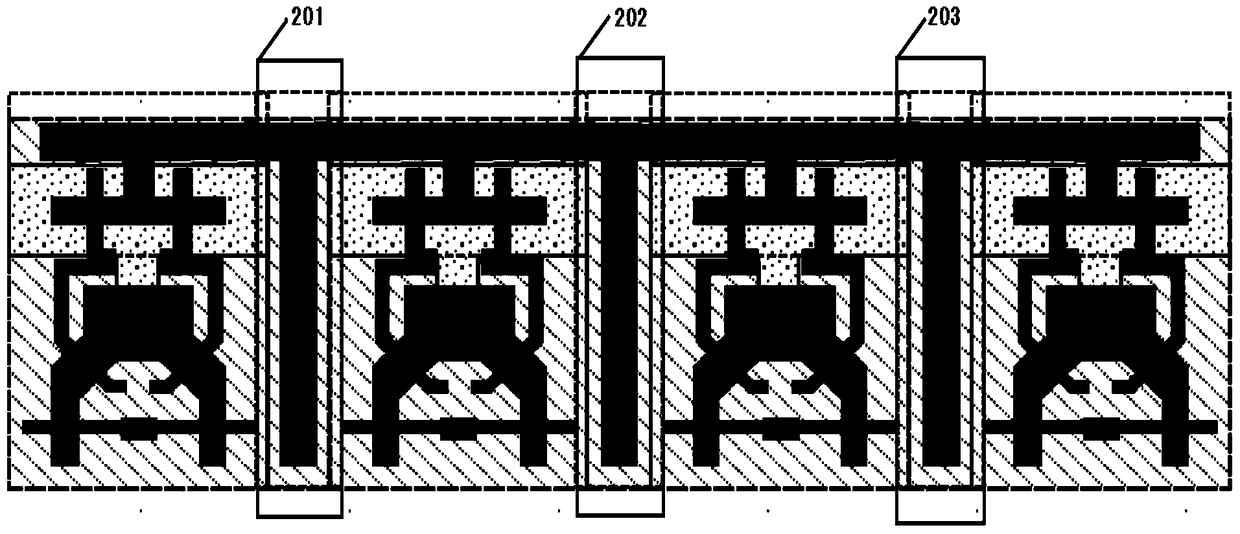
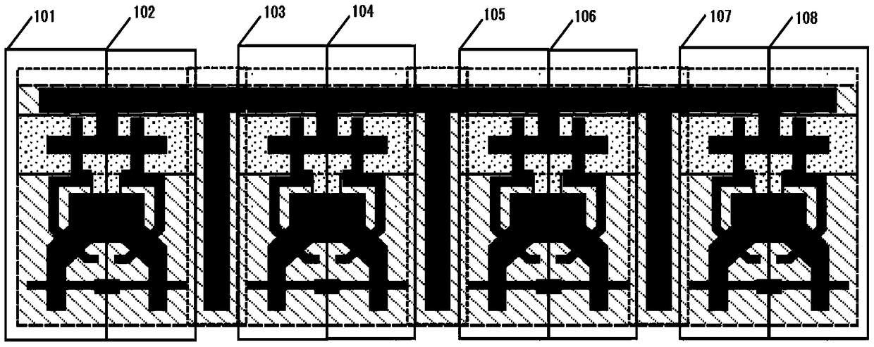
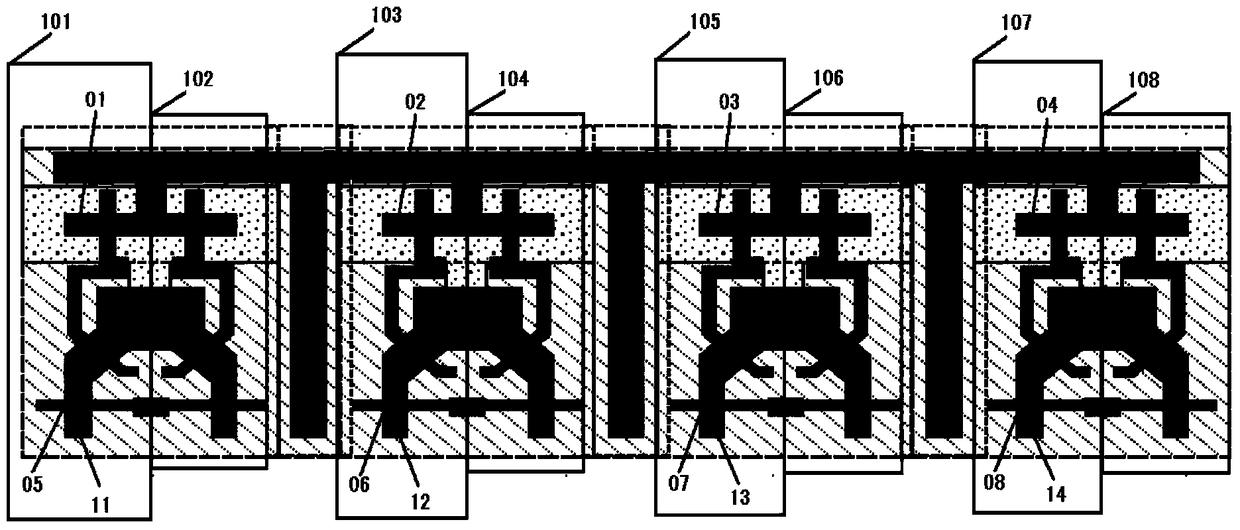
[0026] The invention overcomes the disadvantage that common DICE memory cells in the ultra-deep sub-micron process will cause multiple storage nodes in the unit to flip under the influence of SEU, and eventually lead to the flipping of common DICE memory cells, and proposes a new well-isolated anti-corrosion The SEU multi-node flip memory cell layout structure can effectively separate all sensitive node pairs in the common DICE memory cell structure and increase the distance between sensitive node pairs. Among them, for PMOS transistors, N-well isolation can effectively stabilize the N-well voltage. Reduces the chance of flipping multiple storage nodes due to parasitic bipolar transistor effects. For NMOS transistors, the N-well isolation effectively shunts the holes generated by incoming particles, reducing the occurrence of multiple storage nodes due to charge sharing effects. The probability of flipping, thereby suppressing the multi-node flipping caused by SEU in the DICE u...


PUM


Abstract

A well-isolated anti-SEU multi-node inversion memory cell layout structure, comprising well isolation regions (201), (202), (203), DICE unit regions (101), (103), (105), (107), DICE units (102), (104), (106), (108). The well isolation region is arranged crosswise between the two DICE cell regions. Compared with the prior art, the present invention further increases the distance between sensitive node pairs while effectively separating all sensitive node pairs in the DICE memory cell structure, and the well isolation structure is also beneficial to reduce the distance between sensitive node pairs. The parasitic bipolar transistor effect and the charge sharing effect greatly suppress the multi-node turnover caused by SEU in the DICE unit, and greatly improve the anti-SEU performance of the radiation-resistant SRAM.

Description

technical field [0001] The invention relates to the technical field of memory cells, in particular to a layout structure of a well-isolated anti-SEU multi-node flip memory cell. Background technique [0002] The single event flip effect refers to the radiation produced by high-energy protons or high-energy neutrons hitting the atomic nucleus and the heavy nuclear particles in cosmic rays, which generate high-density charges, which cause the state change of the internal nodes of the storage unit, thereby causing the storage data of the storage unit to flip , this effect is the result of the action of a single particle, commonly known as the Single Event Upset Effect (SEU). [0003] For SRAM, according to the single event effect analysis, the most sensitive place to single event is the memory unit body, because once a single event hits any sensitive node in the memory body, the storage state can be changed. In a conventional CMOS SRAM memory cell, the nodes that store informa...

Claims


Application Information

Patent Timeline
Patent Type & Authority Patents(China)
IPC IPC(8): H01L27/11
CPCH10B10/12
Inventor 赵元富刘皓陆时进刘琳岳素格李鹏张晓晨李阳
Owner BEIJING MXTRONICS CORP
Why Eureka
Try Eureka