An end-fire antenna device mounted on a silicon substrate in the terahertz band

A technology of end-fire antenna and silicon substrate, which is applied in the field of end-fire antenna on terahertz silicon substrate, which can solve the problems of limited radiation area and radiation efficiency of on-chip antenna, failure to meet antenna gain requirements, and reduced radiation efficiency. Achieve the effect of reducing cost, improving antenna efficiency, and small size

Inactive Publication Date: 2018-10-09
INST OF ELECTRONICS ENG CHINA ACAD OF ENG PHYSICS
View PDF4 Cites 1 Cited by
  • Summary
  • Abstract
  • Description
  • Claims
  • Application Information

AI Technical Summary

Problems solved by technology

[0003] However, in the existing low-cost silicon-based semiconductor process, the substrate generally has a low resistivity (usually 10Ω.cm), and the energy radiated by the antenna to the space is more through the low-resistance path of the substrate, resulting in gain decline
At the same time, the substrate usually also has a high dielectric constant (ε r =11.9), resulting in the radiation power of the antenna being confined inside the substrate instead of being radiated to free space, which further reduces the radiation efficiency
[0004] Moreover, the on-chip antenna is limited by the radiation area and radiation efficiency, and its gain is often at a very low level (usually less than 0dB), which cannot meet the requirements for high antenna gain.
In order to reduce the influence of the substrate on the antenna radiation, it is usually possible to reduce the thickness of the substrate to 1 / 4λ g (λ g It is a method below the dielectric wavelength), but when the frequency reaches above 300GHz, the thickness of the substrate needs to be reduced to below 40um, resulting in a decrease in chip strength and easy damage

Method used


Image

  • An end-fire antenna device mounted on a silicon substrate in the terahertz band
  • An end-fire antenna device mounted on a silicon substrate in the terahertz band
  • An end-fire antenna device mounted on a silicon substrate in the terahertz band

Examples


specific Embodiment approach

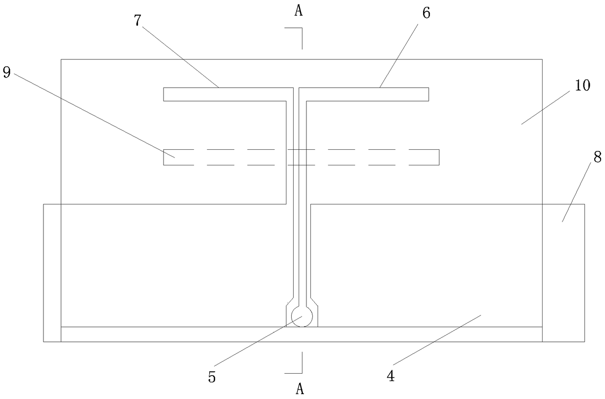
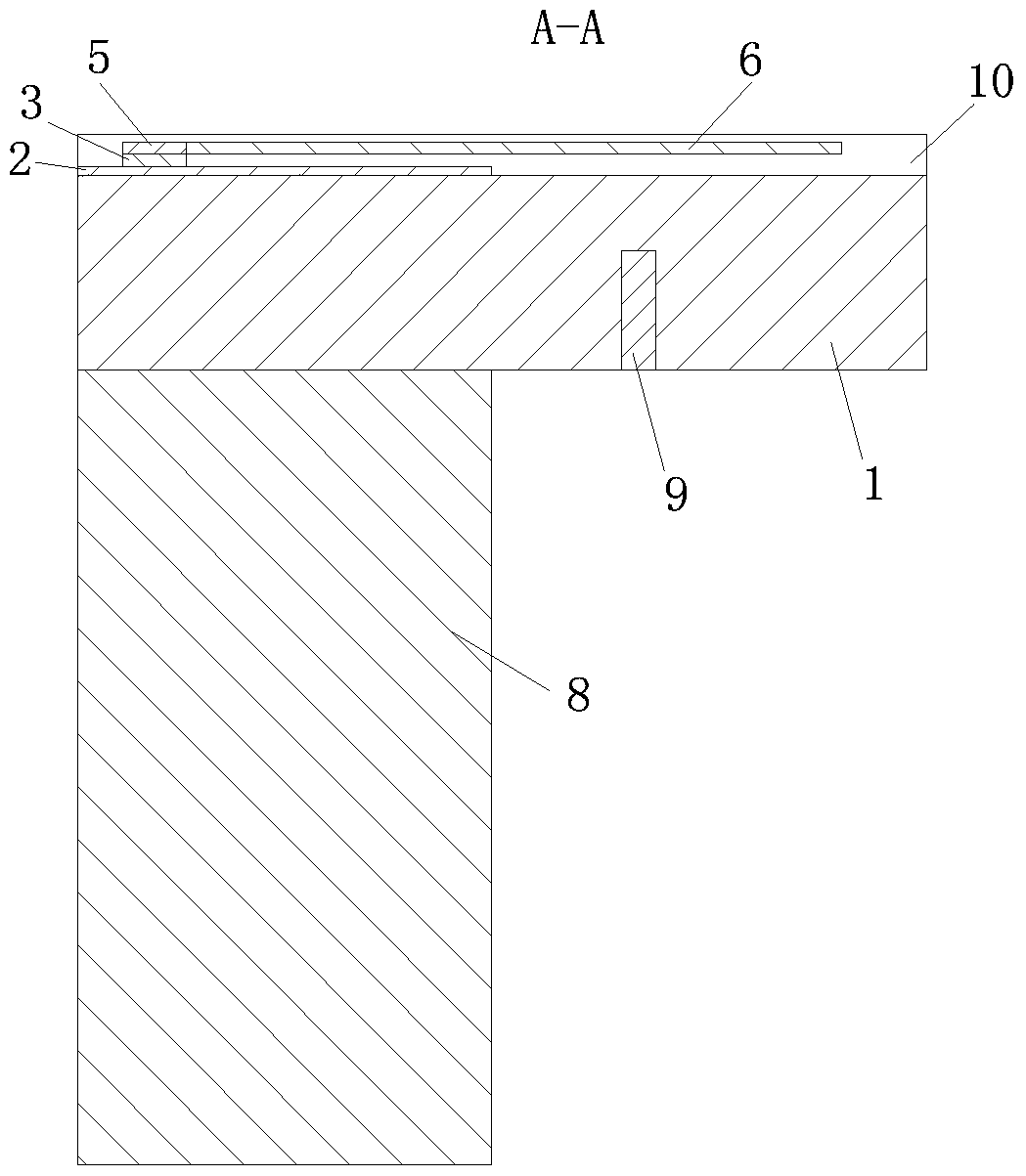
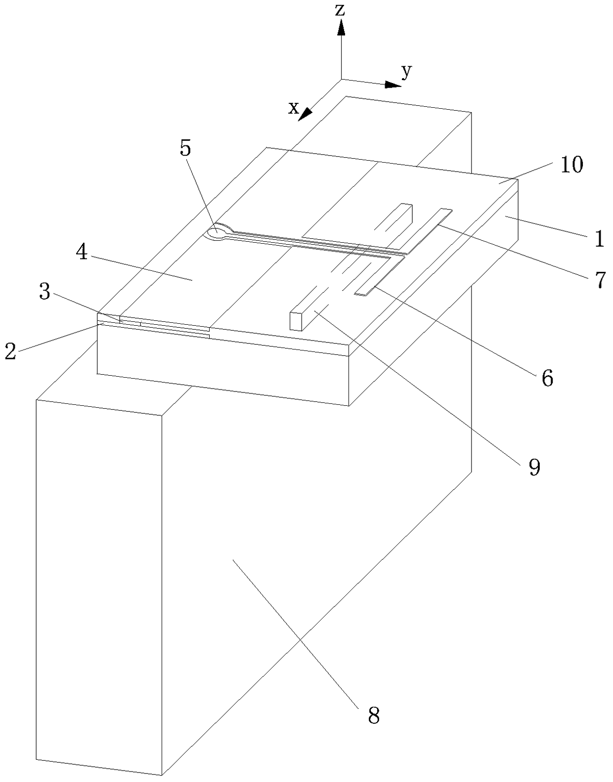
[0025] Such as Figure 1-3 As shown, a specific implementation of this example is:

[0026] An end-fire antenna device mounted on a silicon substrate in the terahertz band, including a substrate 1, wherein: the upper end surface of the substrate 1 is provided with SiO 2 Layer 10, the SiO 2 Layer 10 is provided with a first metal layer 2, a metal block 3, and a second metal layer 4, and the first metal layer 2 is set on the SiO 2 The inner bottom surface of the layer 10, the first metal layer 2 is provided with a metal block 3, the upper end surface of the metal block 3 is provided with a second metal layer 4, the first metal layer 2 and the second metal layer 4 parallel, the upper end surface of the metal block 3 is provided with a feed end 5, the feed end 5 is connected to a balun 6, the second metal layer 4 is connected to a dipole 7, the balun 6, The dipoles 7 are respectively parallel to the substrate 1, and the balun 6 and the dipole 7 are on the same side of the feedi...


PUM

PropertyMeasurementUnit
electrical resistivityaaaaaaaaaa
relative permittivityaaaaaaaaaa

Abstract

The invention discloses a terahertz waveband silicon-chip-loaded end-on-fire antenna apparatus. The apparatus comprises a substrate, the upper end surface of the substrate is provided with a SiO2 layer, a first metal layer, a metal block, and a second metal layer are arranged in the SiO2 layer, the first metal layer is arranged on the inner bottom surface of the SiO2 layer, the first metal layer is provided with the metal block, the upper end surface of the metal block is provided with a second metal layer, the first metal layer is parallel to the second metal layer, the upper end surface of the metal block is provided with a feeding terminal, the feeding terminal is connected with a balun, the second metal layer is connected with a dipole, the balun and the dipole are parallel to the substrate, the balun and the dipole are arranged at the same side of the feeding terminal, and the feeding terminal, the balun, and the dipole are all arranged in the SiO2 layer. According to the apparatus, the absorption of radiation energy of an antenna by the substrate is reduced, the apparatus is fully compatible with the mainstream CMOS technology and applicable to silicon chips with various resistivities, extra impedance match parts are not needed, and the apparatus is advantaged by simple structure, small dimension, high efficiency, and high gain.

Description

technical field [0001] The invention belongs to the field of electrical technology, and in particular relates to a terahertz silicon substrate-mounted end-fire antenna. Background technique [0002] The antenna, as the first element of the receiving end and the last element of the transmitting end, must be connected to the circuit, so in order to ensure maximum power transmission, impedance matching is an essential link. Furthermore, since the antennas are implemented on conventional PCBs, gold wire bonding is used to connect them to the integrated circuits, which can greatly affect the matching, especially in the terahertz band, where the reliability of gold wire bonding and other connection methods is low. In contrast, the on-chip antenna can be integrated with the front-end circuit at one time to solve the above problems. [0003] However, in the existing low-cost silicon-based semiconductor process, the substrate generally has a low resistivity (usually 10Ω.cm), and the...

Claims


Application Information

Patent Timeline
Patent Type & Authority Patents(China)
IPC IPC(8): H01Q1/22H01Q1/38H01Q1/50H01Q19/185
CPCH01Q1/2283H01Q1/38H01Q1/50H01Q19/185
Inventor 邓小东熊永忠
Owner INST OF ELECTRONICS ENG CHINA ACAD OF ENG PHYSICS
Why Eureka
Try Eureka