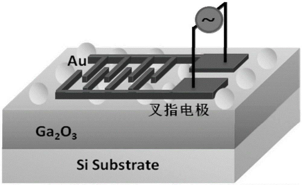
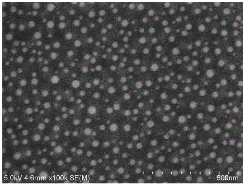
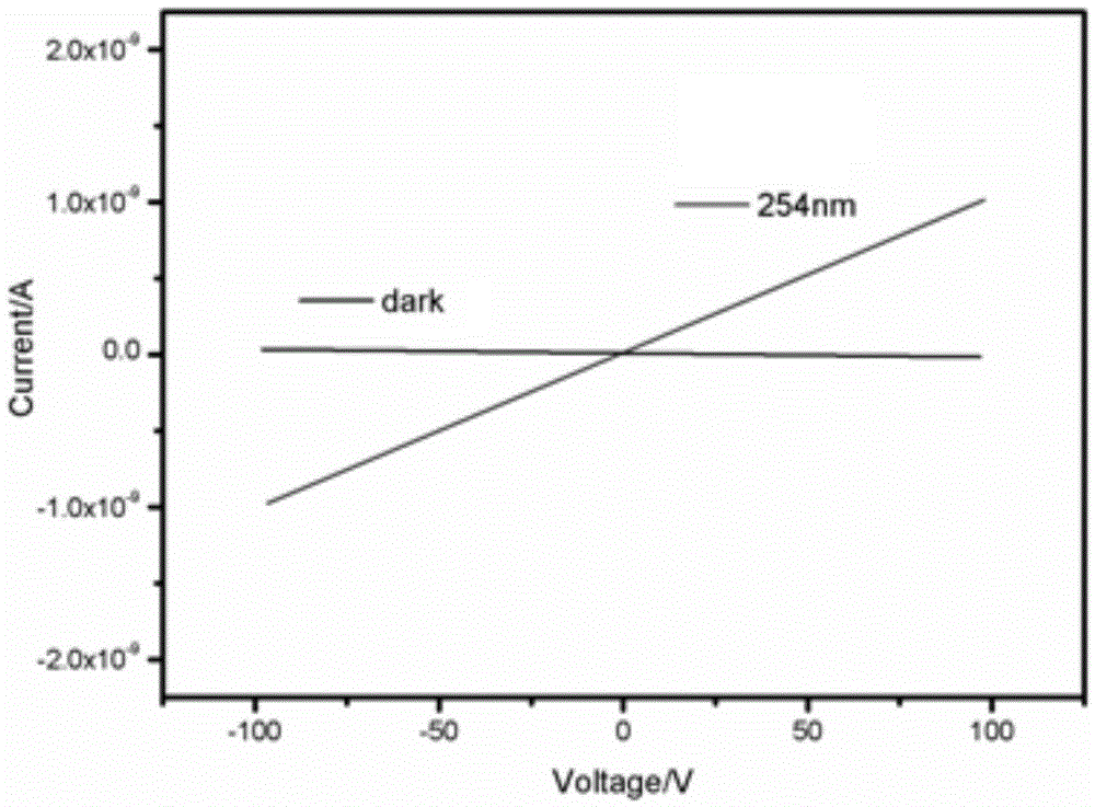
Ultraviolet detection device based on gold nanoparticle enhanced gallium oxide thin film and preparation method thereof
A gold nanoparticle and gold nanoparticle technology, applied in the field of ultraviolet detection devices, can solve the problems of fragile, bulky, etc., and achieve the effects of stable performance, improved sensitivity, and strong process controllability
- Summary
- Abstract
- Description
- Claims
- Application Information
AI Technical Summary
Problems solved by technology
Method used
Image
Examples
Embodiment 1
[0029] Proceed as follows:
[0030] 1. Pretreatment of n-type Si substrate: put n-type Si substrate into V(HF):V(H 2 o 2 )=1:5 solution soaked to remove the natural oxide layer, then ultrasonic cleaning with acetone, ethanol and deionized water respectively, and vacuum drying;
[0031] 2. Place the target and substrate: put the Ga 2 o 3 The target is placed on the target stage of the RF magnetron sputtering system, and the n-type Si substrate processed in step 1) is fixed on the sample holder and put into the vacuum chamber;
[0032] 3. Ga 2 o 3 Thin film deposition process: first evacuate the chamber, heat the n-type Si substrate, pass in argon gas, and adjust the pressure in the vacuum chamber; among them, Ga 2 o 3 The distance between the target and the n-type Si substrate is set to 5 cm, the sputtering power is 60 W, and the deposition time is 1 hour;
[0033] 4. The preparation process of gold nanoparticles: the chamber is first evacuated, and the Ga obtained in h...
Embodiment 2
[0037] Steps (1), (2) and (5) are all the same as in Example 1. In step 3, the chamber is first evacuated, the n-type Si substrate is heated, and argon gas is introduced to adjust the pressure in the vacuum chamber; wherein, Ga 2 o 3 The distance between the target and the n-type Si substrate is set to 5 cm, the sputtering power is 70W, and the deposition time is 1 hour; in step 4, the chamber is first evacuated, the n-type Si substrate is heated, and argon gas is introduced. Adjust the pressure in the vacuum chamber; wherein, the distance between the gold target and the n-type Si substrate is set to 5 cm, the sputtering power is 50 W, and the deposition time is 10 seconds; then the gold film is transferred to a high-temperature furnace for annealing to obtain For gold nanoparticles, the annealing temperature is 450° C., and the annealing time is 1 hour.
[0038] A voltage is applied across the interdigitated electrode of the gold nanoparticle-enhanced gallium oxide film to ...
Embodiment 3
[0040] Steps (1), (2) and (5) are all the same as in Example 1. In step 3, the chamber is first evacuated, the n-type Si substrate is heated, and argon gas is introduced to adjust the pressure in the vacuum chamber; wherein, Ga 2 o 3 The distance between the target and the n-type Si substrate is set to 5 cm, the sputtering power is 70W, and the deposition time is 1 hour; in step 4, the chamber is first evacuated, the n-type Si substrate is heated, and argon gas is introduced. Adjust the pressure in the vacuum chamber; wherein, the distance between the gold target and the n-type Si substrate is set to 5 cm, the sputtering power is 60W, and the deposition time is 15 seconds; then the gold film is transferred to a high-temperature furnace for annealing to obtain For gold nanoparticles, the annealing temperature is 450° C., and the annealing time is 1 hour.
[0041] A voltage is applied across the interdigitated electrode of the gold nanoparticle-enhanced gallium oxide film to m...
PUM
| Property | Measurement | Unit |
|---|---|---|
| thickness | aaaaa | aaaaa |
| interdigital gap | aaaaa | aaaaa |
Abstract
Description
Claims
Application Information
 - R&D
- Intellectual Property
- Life Sciences
- Materials
- Tech Scout
- Unparalleled Data Quality
- Higher Quality Content
- 60% Fewer Hallucinations
Browse by: Latest US Patents, China's latest patents, Technical Efficacy Thesaurus, Application Domain, Technology Topic, Popular Technical Reports.
© 2025 PatSnap. All rights reserved.Legal|Privacy policy|Modern Slavery Act Transparency Statement|Sitemap|About US| Contact US: help@patsnap.com


