Establishment and application of mastocyte-macrophage-coculture-based microfluidic chip
A microfluidic chip, chip technology, applied in tissue cell/virus culture devices, animal cells, vertebrate cells, etc., can solve problems such as risks that cannot be ignored, unfavorable diagnosis and treatment of allergic diseases, etc.
- Summary
- Abstract
- Description
- Claims
- Application Information
AI Technical Summary
Problems solved by technology
Method used
Image
Examples
Embodiment 1
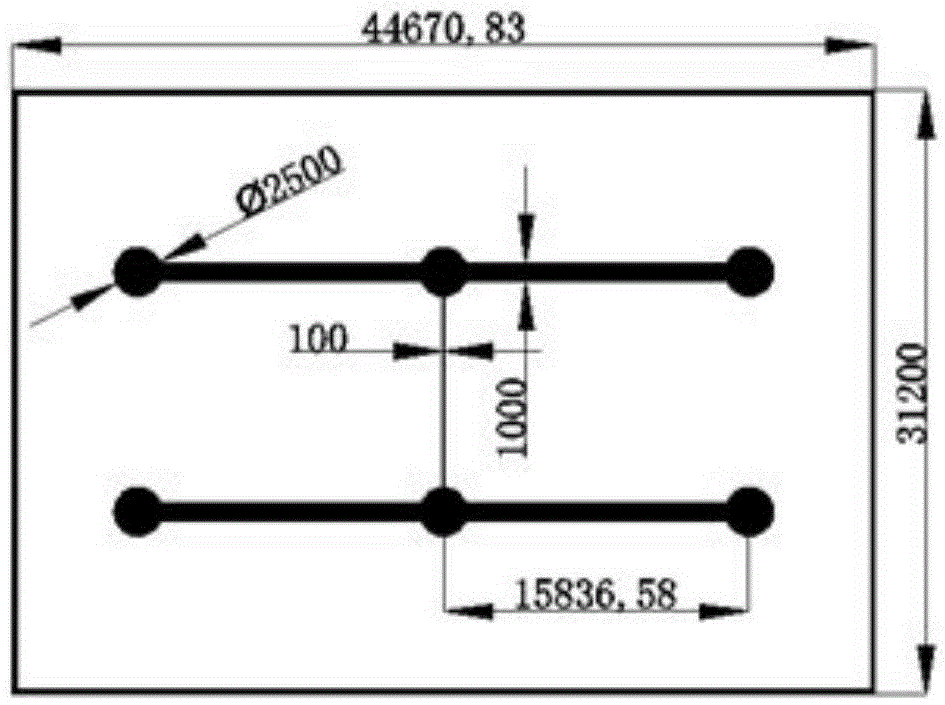
[0033] Example 1 Microfluidic chip physical map
[0034] The physical picture of the microfluidic chip is as follows figure 1 As shown, the specific operation is as follows:
[0035] (1) The first part is the main structure of the chip - the PDMS flow channel layer, with a total length of 44670.83 μm, a width of 31200 μm, and a thickness of 4 mm; two long DC channels with a width of 1000 μm and a length of 31673.16 μm are designed on the chip, and the two ends are respectively equipped with diameter The entrance and exit holes are 2500μm.
[0036] (2) A capillary channel with a length of 10 mm and a width of 100 μm is connected between the two channels.
[0037] (3) Open holes with a diameter of 2 mm are provided at both ends of the capillary to facilitate the insertion of the miniature reference electrode.
[0038] (4) Four sets of gold electrodes are electroplated and integrated on the bottom surface of the cell chip, and a three-electrode system is formed with a plug-in...
Embodiment 2
[0040] Example 2 Dimensions of the gold-plated layer of the microfluidic chip
[0041] Such as figure 2 As shown, the specific operation is as follows:
[0042] (1) Electroplate four groups of gold electrodes on its surface, and the diameter of each working electrode is 1000 μm.
[0043] (2) The guide wire with a diameter of 500 μm connects the working electrode and the gold finger (fixed by the electrode clamp) with a width of 4000 μm on the edge of the chip. In front of the working electrode is an electroplated gold layer (counter electrode) with a half-circle width of 1000 μm. It is also connected to the gold finger on the edge of the chip by a 500μm wide plating wire.
Embodiment 3
[0044] Example 3 Schematic diagram of microfluidic chip assembly
[0045] The entire microfluidic chip was fabricated using a soft lithography method, using polydimethylsiloxane as the main material, which has the characteristics of good biocompatibility and gas permeability (such as image 3 ). The specific operation is as follows:
[0046] (1) Produce SU-8 negative glue (SU82075) master plate on the cleaned silicon wafer by standard photolithography process, and complete the basic production after pre-baking, mask covering, UV exposure, post-baking and developing the master plate .
[0047] (2) Secondly, the PDMS substrate containing microchannels was made by casting method. After the mold was hardened at 65°C for 5 minutes, the PDMS prepolymer and crosslinking agent (mass ratio: 10:1) After mixing evenly, pour it into a mold and dry it in an oven at 80°C for 2 hours.
[0048] (3) After the polymerization is completed, the PDMS is peeled off from the mold, and holes such...
PUM
| Property | Measurement | Unit |
|---|---|---|
| diameter | aaaaa | aaaaa |
Abstract
Description
Claims
Application Information
 - R&D Engineer
- R&D Manager
- IP Professional
- Industry Leading Data Capabilities
- Powerful AI technology
- Patent DNA Extraction
Browse by: Latest US Patents, China's latest patents, Technical Efficacy Thesaurus, Application Domain, Technology Topic, Popular Technical Reports.
© 2024 PatSnap. All rights reserved.Legal|Privacy policy|Modern Slavery Act Transparency Statement|Sitemap|About US| Contact US: help@patsnap.com


