High luminous efficiency light emitting diode epitaxial wafer and preparation method thereof

A technology of light-emitting diodes and high luminous efficiency, which is applied in the direction of electrical components, circuits, semiconductor devices, etc., and can solve the problems of the degree of electronic leakage and the decrease of luminous efficiency of LED chips

Active Publication Date: 2017-12-15
HC SEMITEK CORP
View PDF10 Cites 0 Cited by
  • Summary
  • Abstract
  • Description
  • Claims
  • Application Information

AI Technical Summary

Problems solved by technology

[0005] As the working current of GaN-based LEDs increases, the current density increases accordingly. In this high current density scenario, the electrons injected into the MQW active layer also increase, resulting in the failure of some electrons to interact with the holes. The multi-quantum well active layer recombines and migrates to the P-type GaN carrier layer, resulting in an increase in the degree of electron leakage, which makes the luminous efficiency of the LED chip decrease under the condition of high current density.

Method used


Image

  • High luminous efficiency light emitting diode epitaxial wafer and preparation method thereof
  • High luminous efficiency light emitting diode epitaxial wafer and preparation method thereof

Examples


Embodiment Construction

[0026] In order to make the object, technical solution and advantages of the present invention clearer, the implementation manner of the present invention will be further described in detail below in conjunction with the accompanying drawings.

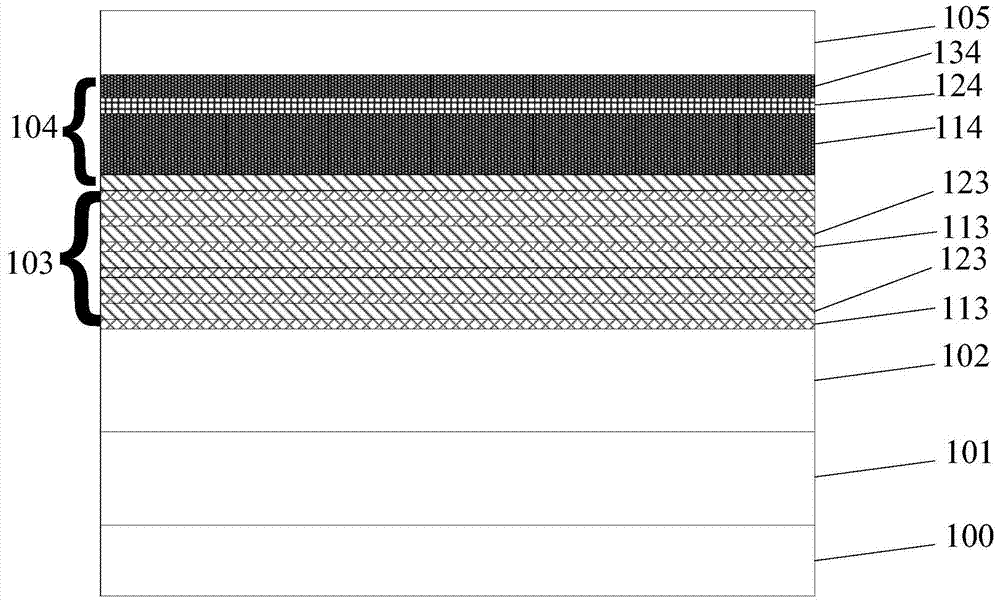
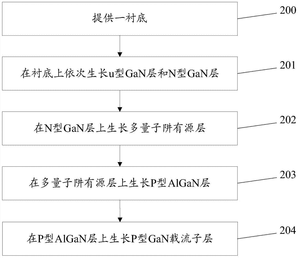
[0027] figure 1 It is a schematic structural diagram of a high-luminous-efficiency light-emitting diode epitaxial wafer provided by an embodiment of the present invention, which is suitable for GaN-based LEDs with blue-green light waves, see figure 1 , the high luminous efficiency light-emitting diode epitaxial wafer includes: a substrate 100, and a u-type GaN layer 101, an N-type GaN layer 102, a multi-quantum well active layer 103, a P-type AlGaN layer 104, As well as the P-type GaN carrier layer 105 , the multi-quantum well active layer 103 includes: a plurality of InGaN well layers 113 and a plurality of GaN barrier layers 123 grown alternately.

[0028] Wherein, the P-type AlGaN layer 104 includes a first P-type AlGaN sub-layer 1...


PUM


Abstract

The invention discloses a light-emitting diode epitaxial wafer with high luminous efficiency and a preparation method thereof, belonging to the field of light-emitting diodes. The high-luminous-efficiency light-emitting diode epitaxial wafer includes: a substrate, and a u-type GaN layer, an N-type GaN layer, a multi-quantum well active layer, a P-type AlGaN layer, and a P-type GaN carrier layer covering the substrate in sequence , the multi-quantum well active layer includes a plurality of InGaN well layers and a plurality of GaN barrier layers grown alternately; the P-type AlGaN layer includes the first P-type AlGaN sublayer, u-type GaN sublayer and the second P-type AlGaN sublayer. It can not only reduce the potential energy required for holes in the P-type GaN carrier layer to cross the P-type AlGaN layer, but also form a quantum state in the u-type GaN sublayer. The potential energy in the P-type GaN carrier layer is lower than that of crossing the P-type The holes with the potential energy required by the AlGaN layer will tunnel into the u-type GaN sub-layer through the quantum tunneling effect, and then be transported into the quantum wells, increasing the hole concentration injected into the multi-quantum well active layer.

Description

technical field [0001] The invention relates to the field of light emitting diodes (English Light Emitting Diode, referred to as LED), in particular to a high luminous efficiency light emitting diode epitaxial wafer and a preparation method thereof. Background technique [0002] LED is known as the most promising green lighting source in the 21st century because of its advantages such as high brightness, low heat, long life, non-toxicity, and recyclability. As the most important category of LEDs, GaN-based LEDs are widely used in many fields. The existing GaN-based LED epitaxial wafer mainly includes a substrate, a buffer layer, an N-type GaN layer, a multi-quantum well active layer, a P-type AlGaN layer, and a P-type GaN carrier layer. [0003] During the working process of GaN-based LEDs, the electrons generated in the N-type GaN layer and the holes generated in the P-type GaN carrier layer migrate to the multi-quantum well active layer under the action of an electric fie...

Claims


Application Information

Patent Timeline
Patent Type & Authority Patents(China)
IPC IPC(8): H01L33/06H01L33/32H01L33/00
CPCH01L33/0075H01L33/06H01L33/32
Inventor 孙玉芹王江波
Owner HC SEMITEK CORP
Why Eureka
Try Eureka