Method for on-line monitoring of preparation of copper indium gallium selenide absorption layer

A copper indium gallium selenide and absorption layer technology, which is applied in the field of online monitoring for preparing a copper indium gallium selenide absorption layer, can solve the problems of limited scope, unrealistic wide application, and difficulty in obtaining a CIGS film with uniform and high crystalline quality. Achieve the effect of improving performance, yield, and high crystal quality

Active Publication Date: 2016-04-20
CHINA ELECTRONIC TECH GRP CORP NO 18 RES INST
View PDF8 Cites 4 Cited by
  • Summary
  • Abstract
  • Description
  • Claims
  • Application Information

AI Technical Summary

Problems solved by technology

However, the monitoring range of a single temperature sensor is limited, it can only accurately reflect a certain local temperature change, and the position of copper selenide on the film surface is random, for the deposition of large-area CIGS film, it is difficult to monitor the temperature sensor Accurately and timely judge the transition point from copper-poor to copper-rich
It is difficult to obtain CIGS thin films with uniform and high crystalline quality even if the abrupt temperature change point is monitored
The X-ray fluorescence spectrometer installed at the winding end of the substrate is only an auxiliary quantitative detection equipment, which can accurately give the composition ratio and thickness of the film, but has a certain hysteresis, and cannot detect the change of the composition ratio during the film growth process online, and cannot monitor Does the CIGS absorber undergo a suitable Cu-rich growth process?
It is also reported in the literature that atomic absorption spectroscopy is used to detect the composition ratio of the absorbing layer film online. This method can only detect the composition ratio of the film in a small range, and it is also not suitable for large-area film deposition, and the use and maintenance costs of the atomic absorption spectroscopy device are high. Wide application in large-area CIGS film batch production lines is unrealistic

Method used


Image

  • Method for on-line monitoring of preparation of copper indium gallium selenide absorption layer
  • Method for on-line monitoring of preparation of copper indium gallium selenide absorption layer
  • Method for on-line monitoring of preparation of copper indium gallium selenide absorption layer

Examples


Embodiment 1

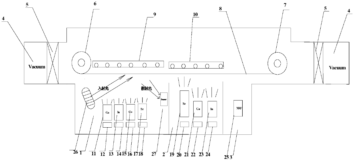
[0027] Example 1 roll-to-roll deposition of large-area CIGS thin films on flexible substrates, see figure 1 .

[0028] The flexible substrate includes metal foil, such as Ti foil, stainless steel sheet, Cu foil, etc., and the thickness of the substrate is 50-100 μm; or it is a plastic substrate, such as polyimide (PI), and the thickness of the substrate is 25-50μm.

[0029] use figure 1 The device shown is in the shape of a rectangular parallelepiped as a whole, and is made of #316 stainless steel plate through seamless welding process; the water-cooling pipeline is seamlessly welded on the surface of the vacuum chamber, and the temperature of the cold water flowing in is about 20°C. The device includes three chambers, a vacuum valve and a vacuum system. The vacuum system 4 is located at both ends of the device, and is used to maintain the vacuum degree of the chamber when the device is coated. A vacuum valve 5 is installed between the first and third chambers and the vacu...

Embodiment 2

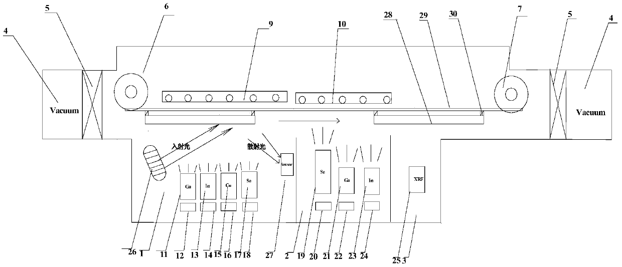
[0035] Embodiment 2 continuously vaporizes and deposits a large area CIGS thin film on a glass substrate, see figure 2 .

[0036] A co-evaporation process is used to continuously deposit a large-area CIGS absorbing layer on the glass substrate / Mo thin film, and the thickness of the glass substrate is 1-3mm. use figure 2The setup shown deposits large area CIGS thin films. The device includes three deposition chambers, a vacuum valve and a vacuum system. The main structure, constituent materials and cooling system of the device are the same as those described in Example 1. The distribution of evaporation sources in the three chambers, the heating system, the temperature control system, the online monitoring device, and the location and layout of the X-ray fluorescence spectrometer are the same as those in Example 1. The difference is that a vapor chamber and a transmission device 29 are installed on the upper part of the first and second deposition chambers. The vapor cham...

Embodiment 3

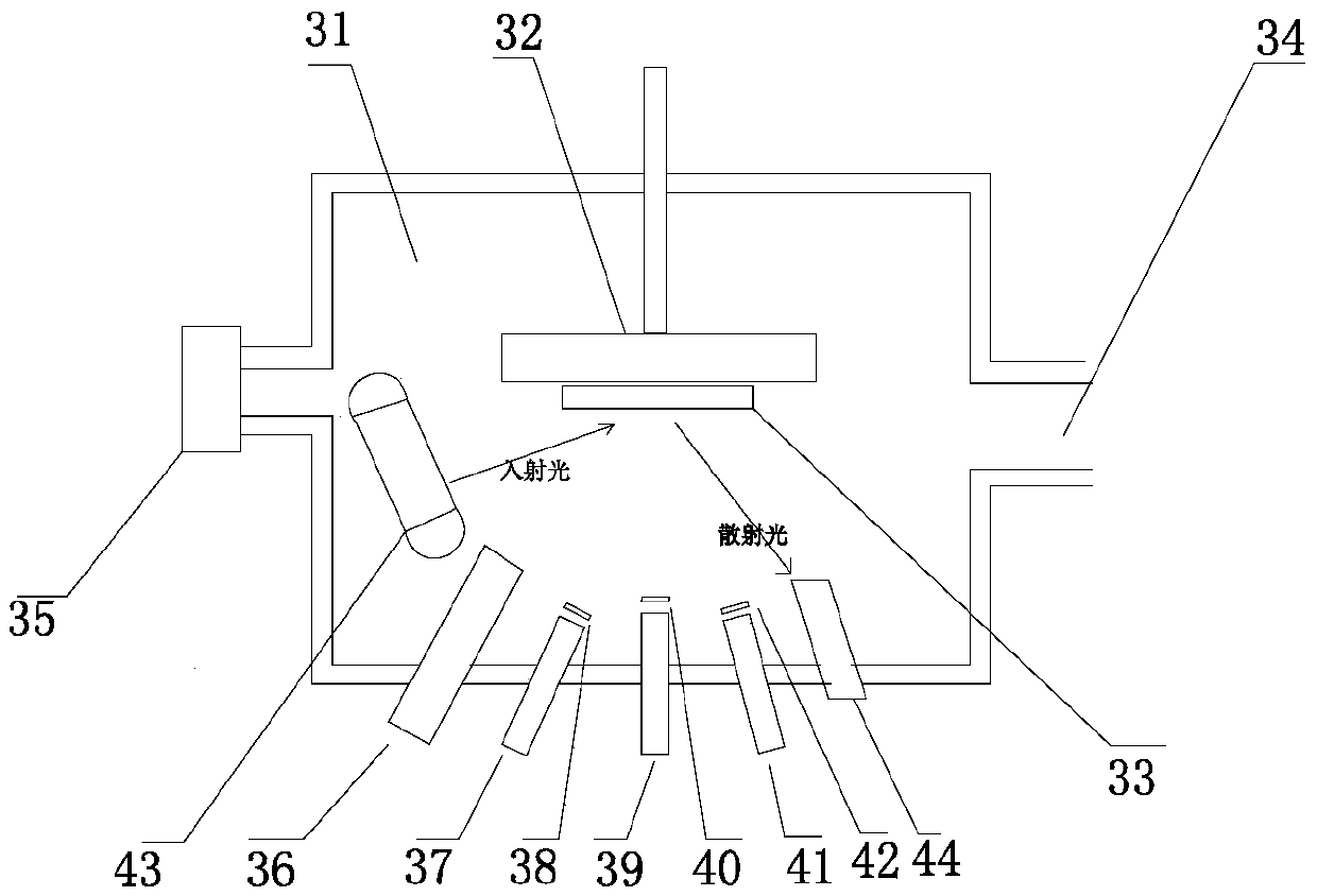
[0039] On-line monitoring and deposition equipment for preparing small-area CIGS thin films in the laboratory of embodiment 3, such as image 3 shown.

[0040] use image 3 The shown device adopts the co-evaporation three-step process to deposit CIGS thin films on flexible or rigid substrates, including flexible substrates such as polyimide and various metal foils, and rigid substrates such as glass . The substrate thickness is 0.05mm-3mm. image 3 The vacuum evaporation chamber 31 in the device is in the shape of a rectangular parallelepiped as a whole, and is made of #316 stainless steel plate through seamless welding process; a water-cooling pipeline is seamlessly welded on the surface of the vacuum chamber, and the temperature of the cold water flowing in is about 20°C. A vacuum pumping system 34 is arranged on the right side of the vacuum chamber, and an ionization gauge 35 is installed on the left side for testing the pressure of the chamber. A substrate heating syst...


PUM


Abstract

The invention discloses a method for on-line monitoring of preparation of a copper indium gallium selenide (CIGS) absorption layer. In a growing process of the CIGS absorption layer, an incandescent lamp is adopted to irradiate a surface of a substrate all the time, a change of the intensity of scattered light from the surface of the substrate is detected through a photosensitive sensor, a change of crystal quality of a surface of a CIGS thin film can be easily monitored on line, not limited by the area of the absorption layer, a transition point of a thin film component from poor copper to rich copper can be judged timely and accurately, the component proportion (Cu / (In+Ga)) in a process of deposition of the CIGS absorption layer is indirectly monitored and controlled, the CIGS absorption layer which is uniform and has relatively high crystal quality is prepared, and the performance and rate of finished products of CIGS thin film solar cells are improved. The CIGS absorption layer can be prepared on a rigid or flexible substrate, and the method provided by the invention can be applied to a laboratory deposition process of the CIGS absorption layer, and can also be used for preparation of a large-area CIGS thin film.

Description

technical field [0001] The invention belongs to the technical field of copper indium gallium selenide thin film solar cells, and in particular relates to an online monitoring method for preparing a copper indium gallium selenide absorbing layer. Background technique [0002] copper indium gallium selenide (Cu(In 1-x , Ga x ) Se 2 , hereinafter referred to as CIGS) thin-film solar cells have the advantages of high photoelectric conversion efficiency, good stability, and strong radiation resistance, and are considered to be one of the most promising photovoltaic devices. In 2014, the efficiency of CIGS thin film solar cells with rigid substrates manufactured by the Stuttgart R&D center (wurthsolar) of German Manz company reached 21.7% (the cell area is about 0.5cm 2 ), surpassing the world record for polysilicon cell efficiency for the first time. In addition, the efficiency of CIGS thin-film solar cells prepared on plastic substrates by the Swiss Federal Institute of Tech...

Claims


Application Information

Patent Timeline
IPC IPC(8): H01L31/18H01L31/032
CPCH01L31/0322H01L31/18Y02E10/541Y02P70/50
Inventor 王赫杨亦桐姚聪乔在祥
Owner CHINA ELECTRONIC TECH GRP CORP NO 18 RES INST
Why Eureka
Try Eureka