
Method to remove photoresist from deep groove and manufacturing method of flash memory

A deep trench, photoresist technology, used in semiconductor/solid-state device manufacturing, electrical components, circuits, etc., can solve the problems of flash memory yield reduction and etching effects, and achieve the effect of improving yield and avoiding short circuits

Active Publication Date: 2016-04-06
SHANGHAI HUAHONG GRACE SEMICON MFG CORP
View PDF4 Cites 4 Cited by
  • Summary
  • Abstract
  • Description
  • Claims
  • Application Information

AI Technical Summary

Problems solved by technology

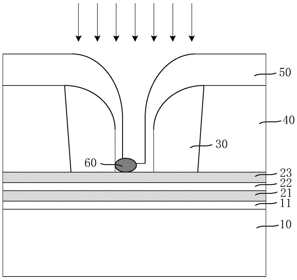
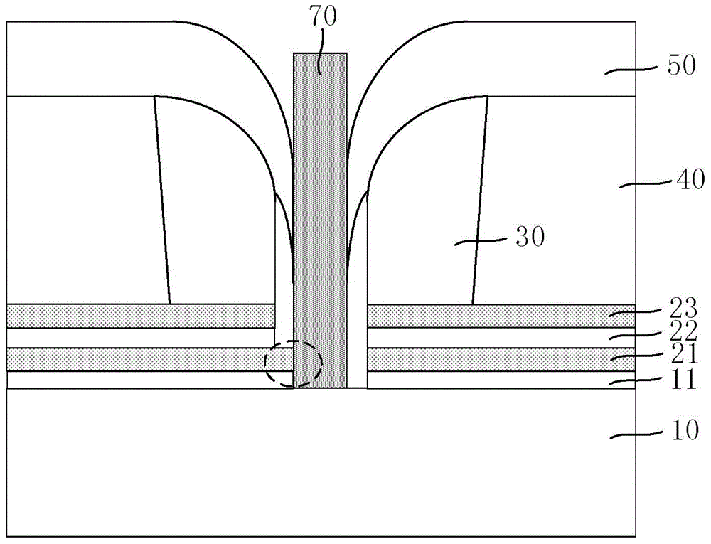
[0004] If there is a short circuit between the floating gate and the source line, it will reduce the yield of the flash memory and cause performance problems of other devices
Therefore, those skilled in the art urgently need to consider how to solve the problem that the remaining photoresist at the bottom corner of the trench affects the etching

Method used


Image

  • Method to remove photoresist from deep groove and manufacturing method of flash memory
  • Method to remove photoresist from deep groove and manufacturing method of flash memory
  • Method to remove photoresist from deep groove and manufacturing method of flash memory

Examples


Embodiment Construction

[0024] The method for removing residual photoresist in deep trenches and the method for manufacturing flash memory of the present invention will be described in more detail below in conjunction with schematic diagrams, wherein a preferred embodiment of the present invention is shown, and it should be understood that those skilled in the art can modify the description herein the present invention while still achieving the advantageous effects of the present invention. Therefore, the following description should be understood as the broad knowledge of those skilled in the art, but not as a limitation of the present invention.

[0025] In the interest of clarity, not all features of an actual implementation are described. In the following description, well-known functions and constructions are not described in detail since they would obscure the invention with unnecessary detail. It should be appreciated that in the development of any actual embodiment, numerous implementation d...


PUM


Abstract

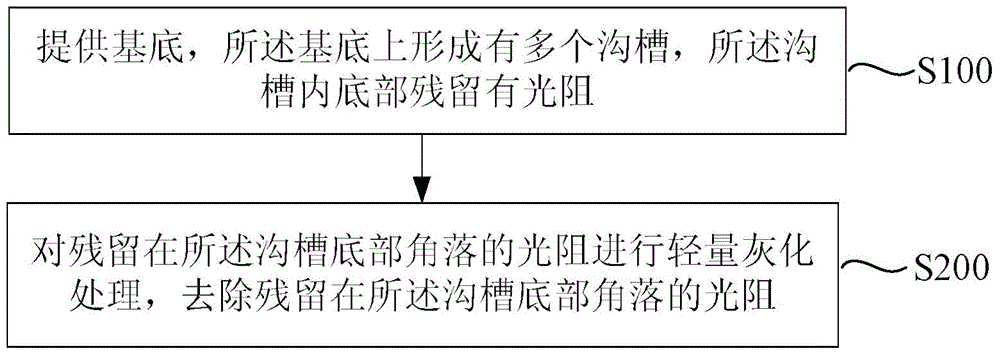
The invention provides a method to remove photoresist from a deep groove and a manufacturing method of a flash memory. Photoresist in the bottom corners of the grooves is ashed into gas by utilizing a light ashing technology, so that the residual photoresist in the bottom corners of the deep groove is removed, and subsequent process can be implemented smoothly. Further, when the flash memory is formed, the residual photoresist at the bottom corners of the deep groove is removed in the light ashing technology, so that subsequent etching process can be carried out smoothly, a floating gate and a source wire formed subsequently are prevented from short circuit, and the yield rate of the flash memory is improved.

Description

technical field [0001] The invention relates to the field of semiconductor manufacturing, in particular to a method for removing residual photoresist in deep grooves and a method for making flash memory. Background technique [0002] With the development of Moore's law in semiconductor technology, the feature size continues to decrease and the integration level continues to increase. In the flash memory 0.12 process, due to the complexity of the integrated circuit design, trenches with high aspect ratio (High AspectRatio) are often encountered in the production process. The depth of this kind of trench is deep and the opening is narrow. The engraving process presents great challenges. [0003] Please refer to figure 1 , figure 1 It is a structural schematic diagram for making flash memory, on the semiconductor substrate 10, a buffer oxide layer 11, a floating gate layer 21 (FloatingGate, FG), a flash memory medium layer 22, a control gate layer 23 (ControlGate, CG), and a...

Claims


Application Information

Patent Timeline
Patent Type & Authority Applications(China)
IPC IPC(8): H01L21/311H01L21/8247H10B41/30
Inventor 苏步春曹子贵孙艳
Owner SHANGHAI HUAHONG GRACE SEMICON MFG CORP
Learn More