


Quick Research
Generate reliable direction feasibility study reports for your R&D in just a few steps.

Technical Q&A
Discover and master advanced knowledge NOW. Basics, ideas, possibilities, all at once.

Find Solutions
As an expert in R&D theories, this can generate solutions to your technical problems instantly.

Evaluate Feasibility
Analyze your overall solution with one click, know your potential R&D risks in advance.

Monitor Landscape
Get weekly tech updates, stay abreast of the latest tech innovations and key insights.
Processing method of PCB line sidewall
A technology of PCB board and processing method, which is applied in the field of processing the side wall of PCB board circuit, can solve the problems of low flatness and large signal loss of the side wall of PCB board circuit, and achieve the effect of ensuring flatness and less signal loss
- Summary
- Abstract
- Description
- Claims
- Application Information
AI Technical Summary
Problems solved by technology
Method used
Image

Examples
Embodiment 1
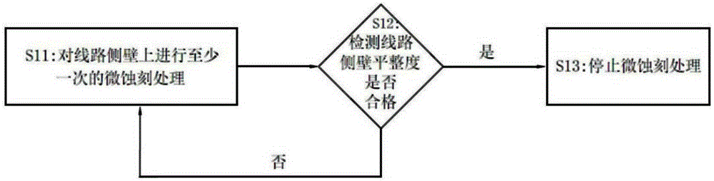
[0046] The present embodiment provides a kind of processing method of circuit side wall of PCB board, as figure 1 shown, including the following steps:
[0047] S11: performing at least one microetching treatment on the circuit sidewall of the substrate;
[0048] S12: Detect whether the flatness of the sidewall of the circuit is qualified; if the flatness of the sidewall of the circuit is qualified, stop the micro-etching (ie step S13); if the flatness of the sidewall of the circuit is unqualified, return to step S11.
[0049] The processing method of the circuit side wall of the PCB board of the present embodiment utilizes the micro-etching solution to carry out multiple treatments to the copper plating on the circuit side wall, and constantly detects the flatness of the circuit side wall. Stop micro-etching when the flatness is qualified, so as to ensure the flatness of the side wall of the PCB board, so that the signal loss of the prepared PCB board is very small during si...
Embodiment 2
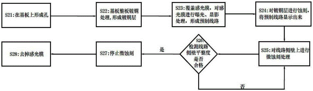
[0072] The present embodiment provides a kind of preparation method of PCB board, comprises the steps:
[0073] Form holes on the substrate of the PCB board;
[0074] forming a copper plating layer on the substrate;
[0075] forming a prefabricated circuit on the surface of the copper plating layer of the substrate;
[0076] The sidewall of the prefabricated circuit is treated by any one of the treatment methods for the sidewall of the PCB circuit provided in Embodiment 1.
[0077] In the PCB preparation method of this embodiment, when the prefabricated circuit is formed on the copper-plated layer of the substrate, any method for processing the side wall of the PCB circuit described in Embodiment 1 is used to process the side wall of the prefabricated circuit, so that the prefabricated The flatness of the side wall of the line is qualified to reduce the signal loss of the PCB board during signal transmission, thereby improving the performance of the signal transmission of th...
Embodiment 3
[0081] This embodiment provides a PCB board with a circuit, and the height difference between the highest convex point and the lowest concave point on the side wall of the circuit is less than or equal to 1 μm, so that the flatness on the circuit side wall of the PCB board meets the requirements, and the PCB board is reduced. Signal loss during signal transmission, thereby improving the signal transmission performance of the PCB board.
[0082] Specifically, the PCB board provided in this embodiment can be prepared by the preparation method described in Embodiment 2, or can be prepared by other preparation methods.
PUM
 Abstract
Description
Claims
Application Information
 - R&D Engineer
- R&D Manager
- IP Professional
- Industry Leading Data Capabilities
- Powerful AI technology
- Patent DNA Extraction
Browse by: Latest US Patents, China's latest patents, Technical Efficacy Thesaurus, Application Domain, Technology Topic, Popular Technical Reports.
© 2024 PatSnap. All rights reserved.Legal|Privacy policy|Modern Slavery Act Transparency Statement|Sitemap|About US| Contact US: help@patsnap.com