Light-emitting device package, manufacturing method thereof, and vehicle lamp and backlight unit including the light-emitting device package

A light-emitting device packaging, light-emitting device technology, applied in the direction of semiconductor devices, electric solid-state devices, electrical components, etc., can solve problems such as the miniaturization limitation of light-emitting devices, and achieve the effect of protecting eyesight, preventing light leakage, and eliminating the packaging process

Active Publication Date: 2018-01-12
SEOUL SEMICONDUCTOR
View PDF8 Cites 0 Cited by
  • Summary
  • Abstract
  • Description
  • Claims
  • Application Information

AI Technical Summary

Problems solved by technology

In addition, the second substrate must be provided to the light emitting device together with the growth substrate, thereby causing limitations in the miniaturization of the light emitting device

Method used


Image

  • Light-emitting device package, manufacturing method thereof, and vehicle lamp and backlight unit including the light-emitting device package
  • Light-emitting device package, manufacturing method thereof, and vehicle lamp and backlight unit including the light-emitting device package
  • Light-emitting device package, manufacturing method thereof, and vehicle lamp and backlight unit including the light-emitting device package

Examples


Embodiment Construction

[0072] Hereinafter, exemplary embodiments of the present invention will be described in detail with reference to the accompanying drawings. The following embodiments are provided by way of illustration in order to fully convey the spirit of the present invention to those skilled in the art to which the present invention pertains. Therefore, the present invention is not limited to the embodiments disclosed herein, and may also be implemented in various forms. In the drawings, the width, length, thickness, etc. of elements may be exaggerated for clarity and descriptive purposes. When an element or layer is referred to as being "disposed over" or "disposed over" another element or layer, it can be "directly disposed over" or "directly disposed on" another element or layer. an element or layer", or intervening elements or layers may be present. Throughout the specification, like reference numerals designate like elements having the same or similar functions.
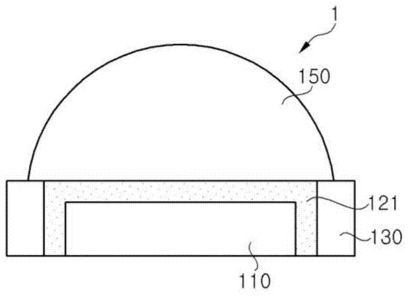
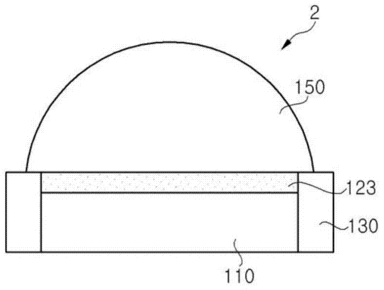
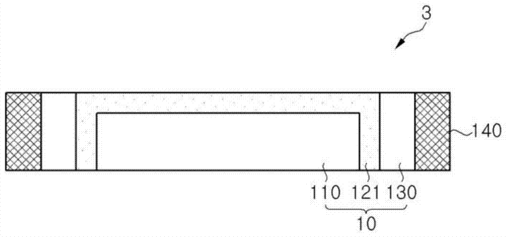
[0073] figure 1 ...


PUM


Abstract

Disclosed are a light emitting device package, a manufacturing method thereof, and a vehicle lamp and a backlight unit including the light emitting device package. The light emitting device package includes a light emitting chip having electrode pads disposed at a lower portion thereof, a wavelength conversion unit covering at least upper and side surfaces of the light emitting chip, and a reflective member covering side surfaces of the light emitting chip. Accordingly, the light emitting device package can be miniaturized without requiring a separate substrate for forming a lens.

Description

technical field [0001] Exemplary embodiments relate to a light emitting device package and a manufacturing method thereof, and a vehicle lamp and a backlight unit including the light emitting device package, and particularly to a small light emitting device package, a method of manufacturing a wafer level light emitting device package, and a light emitting device package including the small light emitting device. Device packages for automotive lamps and backlight units. Background technique [0002] A light emitting diode is an inorganic semiconductor device capable of emitting light through the recombination of electrons and holes, and is used in various fields including displays, car lights, general lighting, and the like. Light emitting diodes have various advantages such as long life, low power consumption, and fast response, and light emitting device packages including such light emitting diodes are expected to replace conventional light sources. Since light emitting d...

Claims


Application Information

Patent Timeline
Patent Type & Authority Patents(China)
IPC IPC(8): H01L33/48
CPCH01L33/486H01L33/50H01L33/60H01L25/0753H01L2924/0002H01L33/14H01L33/20H01L33/36H01L33/58H01L2924/00H01L27/156H01L33/0095H01L33/502H01L2933/0016H01L2933/0033H01L2933/0041H01L2933/0058
Inventor 郑井和郑丞晧黄成基
Owner SEOUL SEMICONDUCTOR
Why Eureka
Try Eureka