Low cost perovskite solar cell being suitable for production
A solar cell and perovskite technology, applied in circuits, photovoltaic power generation, electrical components, etc., can solve the problems of low conversion efficiency, insufficient conversion efficiency, and inability to mass-produce, and achieve the effect of improving the conversion rate
- Summary
- Abstract
- Description
- Claims
- Application Information
AI Technical Summary
Problems solved by technology
Method used
Image
Examples
Embodiment 1
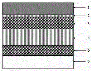
[0027] 1) Use fluorine tin oxide (FTO, fluorinated opedtinoxide) conductive glass as the light-transmitting / transparent electrode layer;
[0028] 2) Prepare a chromium sulfide film on FTO by physical vapor deposition method, with a thickness of 15 nanometers;
[0029] 3) Prepare light absorbing layer:
[0030] a. prepare PbI2 solution, concentration is 3.0Mol / L, solvent is dimethylformamide;
[0031] b. Prepare CH3NH3I solution: the concentration is 5 mg / mL, and the solvent is isopropanol;
[0032] In-situ synthesis of perovskite materials by solution method: spin-coat PbI2 solution on the electron transport layer first, dry it and soak it in CH3NH3I solution to grow perovskite materials, and obtain perovskite light-absorbing layer; thickness 53nm;
[0033] 4) Preparation of electron absorbing layer
[0034] The chlorobenzene solution of PCBM is used to spin-coat on the light-absorbing layer, and dry to obtain an electron-absorbing layer with a thickness of 145nm;
[0035]...
Embodiment 2
[0041] 1) ITO (Indium Tin Oxides) conductive glass is used as the light-transmitting / transparent electrode layer;
[0042] 2) Manganese sulfide film was prepared on ITO by physical vapor deposition method, with a thickness of 10 nanometers;
[0043] 3) Prepare light absorbing layer:
[0044] a. prepare PbI2 solution, concentration is 2.3Mol / L, and solvent is dimethylformamide;
[0045] b. Prepare CH3NH3I solution: the concentration is 7.5mg / mL, and the solvent is isopropanol;
[0046] In-situ synthesis of perovskite materials by solution method: spin-coat PbI2 solution on the electron transport layer first, dry it and soak it in CH3NH3I solution to grow perovskite materials, and obtain perovskite light-absorbing layer; thickness 430nm;
[0047] 4) Preparation of electron absorbing layer
[0048] The chlorobenzene solution of PCBM is used to spin-coat the light-absorbing layer, and dry to obtain an electron-absorbing layer with a thickness of 83nm;
[0049] 5) Preparation o...
Embodiment 3
[0055] 1) ITO conductive glass is used as the light-transmitting / transparent electrode layer;
[0056] 2) Manganese sulfide film was prepared on ITO by thermal evaporation method, with a thickness of 38 nanometers;
[0057] 3) Prepare light absorbing layer:
[0058] a. Prepare PbI2 solution, the concentration is 1.5Mol / L, and the solvent is dimethylformamide;
[0059] b. Prepare CH3NH3I solution: the concentration is 8.5 mg / mL, and the solvent is isopropanol;
[0060] In-situ synthesis of perovskite materials by solution method: spin-coat PbI2 solution on the electron transport layer first, dry it and soak it in CH3NH3I solution to grow perovskite materials, and obtain perovskite light-absorbing layer; thickness 491nm;
[0061] a. Prepare PbI2 solution, the concentration is 1.5Mol / L, and the solvent is dimethylformamide;
[0062] b. Prepare CH3NH3I solution: the concentration is 8.5 mg / mL, and the solvent is isopropanol;
[0063] In-situ synthesis of perovskite materials b...
PUM
 Abstract
Description
Claims
Application Information
 - R&D
- Intellectual Property
- Life Sciences
- Materials
- Tech Scout
- Unparalleled Data Quality
- Higher Quality Content
- 60% Fewer Hallucinations
Browse by: Latest US Patents, China's latest patents, Technical Efficacy Thesaurus, Application Domain, Technology Topic, Popular Technical Reports.
© 2025 PatSnap. All rights reserved.Legal|Privacy policy|Modern Slavery Act Transparency Statement|Sitemap|About US| Contact US: help@patsnap.com

