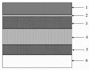
PIN heterojunction solar cell
A solar cell and heterojunction technology, applied in the field of solar cells
- Summary
- Abstract
- Description
- Claims
- Application Information
AI Technical Summary
Problems solved by technology
Method used
Image
Examples
Embodiment 1
[0032] 1) ITO conductive glass is used as the light-transmitting / transparent electrode layer;
[0033] 2) According to the molar ratio of 2:1:6, a mixed solution of nickel acetone caproate, lithium acetate, and magnesium acetate tetrahydrate was prepared, spin-coated on the light-transmitting / transparent electrode layer, and dried at 350°C to prepare the electron Transport layer; thickness 99nm;
[0034] 3) Prepare light absorbing layer:
[0035] a. Prepare PbI2 solution, the concentration is 1.5Mol / L, and the solvent is dimethylformamide;
[0036] b. Prepare CH3NH3I solution: the concentration is 8.5 mg / mL, and the solvent is isopropanol;
[0037] In-situ synthesis of perovskite materials by solution method: first spin-coat PbI2 solution on the electron transport layer, after drying, soak in CH3NH3I solution to grow perovskite materials, and obtain perovskite light-absorbing layer. Thickness 492nm;
[0038] 4) Preparation of electron absorbing layer
[0039] Add graphite...
Embodiment 2
[0047] 1) Aluminum zinc oxide AZO conductive glass is used as the light-transmitting / transparent electrode layer;
[0048] 2) According to the molar ratio of 1:1:3, a mixed solution of nickel acetone caproate, lithium acetate, and magnesium acetate tetrahydrate was prepared, spin-coated on the light-transmitting / transparent electrode layer, and dried at 400°C to prepare the electron Transport layer; thickness 84nm;
[0049] 3) Prepare light absorbing layer:
[0050] a. Prepare PbI2 solution, the concentration is 0.5Mol / L, and the solvent is dimethylformamide;
[0051] b. Prepare CH3NH3I solution: the concentration is 10 mg / mL, and the solvent is isopropanol;
[0052] In-situ synthesis of perovskite materials by solution method: first spin-coat PbI2 solution on the electron transport layer, after drying, soak in CH3NH3I solution to grow perovskite materials, and obtain perovskite light-absorbing layer. Thickness 495nm;
[0053] 4) Preparation of electron absorbing layer
...
Embodiment 3
[0062] 1) Use fluorine tin oxide (FTO, fluorinated opedtinoxide) conductive glass as the light-transmitting / transparent electrode layer;
[0063] 2) According to the molar ratio of 2:1:3, a mixed solution of nickel acetone caproate, lithium acetate, and magnesium acetate tetrahydrate was prepared, spin-coated on the light-transmitting / transparent electrode layer, and dried at 360°C to prepare the electron Transport layer; thickness 87nm;
[0064] 3) Prepare light absorbing layer:
[0065] a. prepare PbI2 solution, concentration is 3.0Mol / L, and solvent is dimethylformamide;
[0066] b. Prepare CH3NH3I solution: the concentration is 5 mg / mL, and the solvent is isopropanol;
[0067] In-situ synthesis of perovskite materials by solution method: spin-coat PbI2 solution on the electron transport layer first, dry it and soak it in CH3NH3I solution to grow perovskite materials, and obtain a perovskite light-absorbing layer with a thickness of 52nm;
[0068] 4) Preparation of elect...
PUM
 Abstract
Description
Claims
Application Information
 - R&D
- Intellectual Property
- Life Sciences
- Materials
- Tech Scout
- Unparalleled Data Quality
- Higher Quality Content
- 60% Fewer Hallucinations
Browse by: Latest US Patents, China's latest patents, Technical Efficacy Thesaurus, Application Domain, Technology Topic, Popular Technical Reports.
© 2025 PatSnap. All rights reserved.Legal|Privacy policy|Modern Slavery Act Transparency Statement|Sitemap|About US| Contact US: help@patsnap.com

