
Fabrication method of circuit board solder mask layer

A manufacturing method and circuit board technology, which are applied in the directions of printed circuit manufacturing, printed circuit, and non-metallic protective layer coating, etc., can solve the problems of speeding up circuit boards, dropping bridges, breaking bridges, etc., so as to improve the firmness and not easily drop bridges , the effect of increasing the binding force

Inactive Publication Date: 2016-02-17
SHENZHEN SUNTAK MULTILAYER PCB
View PDF7 Cites 9 Cited by
  • Summary
  • Abstract
  • Description
  • Claims
  • Application Information

AI Technical Summary

Problems solved by technology

[0006] In this way, for 50μm (50μm is already the limit capacity of bridge width) ≤ solder mask bridge width ≤ 75μm, due to insufficient exposure energy, ink refractive index and other factors, it is easy to appear bridge drop and broken bridge problems during development.
If you simply increase the exposure energy or prolong the exposure time, it is easy to cause overexposure
If the method of simply reducing the spray pressure of the liquid medicine during development, speeding up the speed of the circuit board passing through the spray development line or reducing the concentration of the developing liquid is easy to appear, the problem of unclean development of the solder resist ink will occur.

Method used


Image

  • Fabrication method of circuit board solder mask layer
  • Fabrication method of circuit board solder mask layer
  • Fabrication method of circuit board solder mask layer

Examples


Embodiment

[0030] Solder Mask Requirements

[0031] Solder resist ink thickness: 10-30μm;

[0032] Solder resist bridge width: 50μm≤solder resist bridge width≤75μm.

[0033] The manufacturing process of the circuit board solder mask layer is as follows:

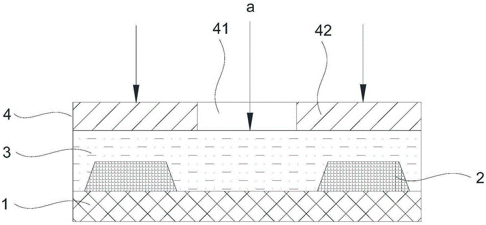
[0034] Cover the solder resist ink with silk screen printing on the surface of the circuit board, and then pre-bake the solder resist ink at 75±5°C for 45 minutes to cure the solder resist ink to ensure that the thickness of the solder resist ink is 8-15 μm after curing.

[0035] Cover the surface of the cured solder resist ink with a film sheet for the first exposure, and the exposure step uses 300-320mj / cm 2 Exposure energy exposure 7s.

[0036] After the first exposure, the circuit board passes through the spray development line with a length of 6m, and the solder resist ink in the unexposed area is washed away by the developing solution; the speed of the circuit board passing through the spray development line is 3.5m / min, and th...


PUM


Abstract

The invention discloses a fabrication method of a circuit board solder mask layer, and relates to the technical field of producing and manufacturing of circuit boards. The fabrication method of the circuit board solder mask layer sequentially comprises the following steps: covering the surface of the circuit board with solder resist ink and pre-baking and curing the solder resist ink; coating the cured solder resist ink on the surface of the circuit board with a film for carrying out first exposure; enabling the circuit board which is exposed once to pass through a spray developer line, and rinsing out the solder resist ink in the unexposed region with a photograph potion; drying the developed circuit board, and then coating with the film which is the same as that in the first exposure for carrying out second exposure; enabling the circuit board which is exposed for the second time to pass through the spray developer line, and rinsing out the solder resist ink in the unexposed region with the photograph potion. According to the method, the binding force of the solder resist ink and the surface of the circuit board can be reinforced; the problems of bridge drop and bridge cutoff of the solder resist ink are overcome; and the capability of the manufacture procedure of a solder mask bridge site is improved.

Description

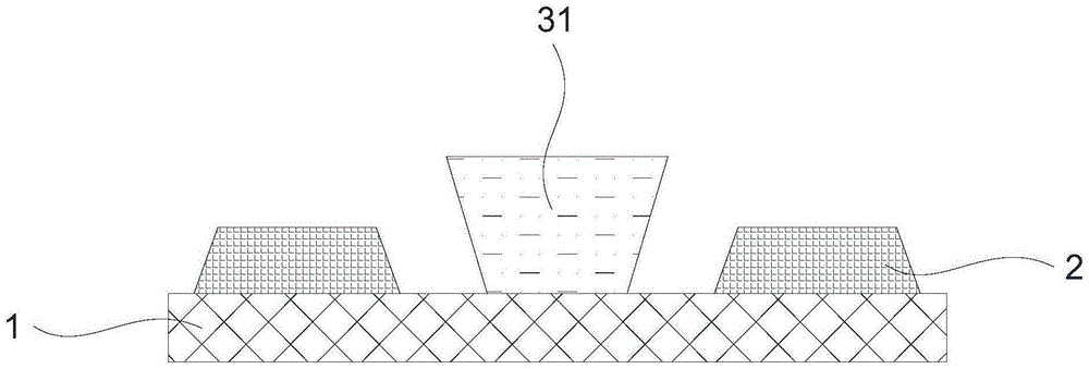
technical field [0001] The invention relates to the technical field of circuit board production and manufacturing, in particular to a method for manufacturing a solder resist layer of a circuit board. Background technique [0002] In the production process of circuit board solder resist ink, after the solder resist ink covers the surface of the circuit board, it needs to be pre-baked and exposed, and then use 2%-3% concentration of Na 2 CO 3 The solution washes away the solder mask from the unexposed areas, leaking out of the pad. [0003] Such as figure 1 , 2 As shown, the circuit board solder resist bridge 31, that is, the solder resist layer 3 located between the IC type pads 2, is called a "solder resist bridge" because of its narrow and long shape, similar to a bridge connecting the solder resist layers at both ends. ". When 50μm≤solder resist bridge width≤75μm, since the solder resist ink has a certain side erosion during development, if the bonding force between ...

Claims


Application Information

Patent Timeline
Patent Type & Authority Applications(China)
IPC IPC(8): H05K3/28
CPCH05K3/282H05K2203/0594
Inventor 王海燕朱拓王自杰
Owner SHENZHEN SUNTAK MULTILAYER PCB
Learn More