
Graphene quantum well optical detector

A photodetector, ene quantum technology, applied in semiconductor devices, electrical components, circuits, etc., can solve problems such as limiting wide application, achieve the effect of large detection sensitivity and improve quantum efficiency

Active Publication Date: 2016-02-17
TSINGHUA UNIV
View PDF4 Cites 1 Cited by
  • Summary
  • Abstract
  • Description
  • Claims
  • Application Information

AI Technical Summary

Problems solved by technology

[0003] At present, the mainstream photodetectors in the medium and long-range light bands, including InSb photodetectors, HgCdTe photodetectors, and quantum well photodetectors, all work at low temperatures (usually lower than 100K), and need to be refrigerated by liquid nitrogen Dewar or circulating refrigerators. , which severely limits their wide application

Method used


Image

  • Graphene quantum well optical detector

Examples


Embodiment Construction

[0013] Embodiments of the present invention are described in detail below, examples of which are shown in the drawings, wherein the same or similar reference numerals designate the same or similar elements or elements having the same or similar functions throughout. The embodiments described below by referring to the figures are exemplary and are intended to explain the present invention and should not be construed as limiting the present invention.

[0014] The graphene quantum well photodetector of the embodiment of the present invention is described below with reference to the accompanying drawings.

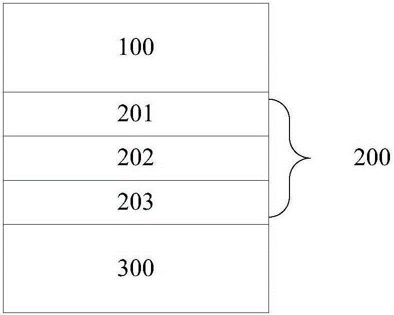
[0015] figure 1 It is a schematic structural diagram of a graphene quantum well photodetector according to an embodiment of the present invention.

[0016] Such as figure 1 As shown, the graphene quantum well photodetector of the embodiment of the present invention includes a first piezoelectric layer 100 , a quantum well layer 200 and a second piezoelectric layer 300 .

[...


PUM


Abstract

The invention discloses a graphene quantum well optical detector. The graphene quantum well optical detector comprises a first piezoelectric layer, a second piezoelectric layer and a quantum well layer, wherein both the first piezoelectric layer and the second piezoelectric layer are made of piezoelectric materials; the quantum well layer is located between the first piezoelectric layer and the second piezoelectric layer and comprises two semiconductor sublayers and a graphene nanoribbon located between the two semiconductor sublayers. The graphene quantum well optical detector has the advantages that the optimal bias voltage of a quantum well is used for making the highest energy level in the quantum well aligned with the boundary of a conduction band to form a maximum output light current, and then highest detection sensitivity is achieved; piezoelectric potential is used for adjusting the bias voltage of the quantum well, so that the quantum efficiency of a single quantum well is improved.

Description

technical field [0001] The invention relates to the field of semiconductors, in particular to a graphene quantum well photodetector. Background technique [0002] Traditional detectors that have developed more maturely in the mid-light to high-light bands include indium telluride (InSb) photodetectors and mercury cadmium telluride (HgCdTe) photodetectors. In the past thirty years, with the development of low-dimensional material technology, a new technology of quantum well photodetector has emerged, and has been developed rapidly and widely used. Compared with other optical technologies, quantum well photodetectors have the advantages of fast response speed, high detection rate, adjustable detection wavelength, strong radiation resistance, etc., and can be used by molecular beam epitaxy (MBE) or metal organic chemical vapor deposition (MOCVD) ) and other advanced technology growth, it is easy to make a high-quality, large-area, and uniform detector array. Among the various...

Claims


Application Information

Patent Timeline
IPC IPC(8): H01L31/09H01L31/028H01L31/0352
CPCH01L31/028H01L31/035236H01L31/035254H01L31/09
Inventor 卢琪伍晓明张进宇吴华强钱鹤余志平
Owner TSINGHUA UNIV
Learn More