High-efficiency perovskite solar cell and preparation method thereof
A solar cell and perovskite technology, applied in circuits, photovoltaic power generation, electrical components, etc., can solve problems such as inability to mass-produce, and achieve the effect of improving time stability and conversion rate
- Summary
- Abstract
- Description
- Claims
- Application Information
AI Technical Summary
Problems solved by technology
Method used
Image
Examples
Embodiment 1
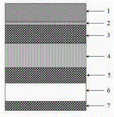
[0028] 1) Use ITO conductive glass as the light-transmitting / transparent electrode layer;
[0029] 2) Using spraying thermal decomposition technology to prepare NiO layer on the surface of conductive glass, thickness 35nm;
[0030] 3) Prepare a mixed solution of nickel acetone hexanoate, lithium acetate, and magnesium acetate tetrahydrate according to the molar ratio of 1:1:5, spin-coat on the transition layer, and dry at 300°C to prepare an electron transport layer with thickness Control at 10nm;
[0031] 4) Preparation of light-absorbing layer:
[0032] a. Prepare PbI2 solution, the concentration is 3.0Mol / L, and the solvent is dimethylformamide;
[0033] b. Preparation of CH3NH3I solution: concentration 5mg / mL, solvent is isopropanol;
[0034] The perovskite material is synthesized in situ by the solution method: the PbI2 solution is spin-coated on the electron transport layer, dried, and then put into the CH3NH3I solution to soak to grow the perovskite material to obtain the perovsk...
Embodiment 2
[0043] 1) Use aluminum-zinc oxide AZO conductive glass as the light-transmitting / transparent electrode layer;
[0044] 2) Using spraying thermal decomposition technology to prepare NiO2 layer on the surface of conductive glass; thickness 50nm;
[0045] 3) Prepare a mixed solution of nickel acetone hexanoate, lithium acetate, and magnesium acetate tetrahydrate in a molar ratio of 1:1:3, spin-coat on the transition layer, and dry at 400°C to prepare an electron transport layer; thickness 60nm;
[0046] 4) Preparation of light-absorbing layer:
[0047] a. Prepare PbI2 solution, the concentration is 0.5Mol / L, the solvent is dimethylformamide;
[0048] b. Preparation of CH3NH3I solution: concentration 10mg / mL, solvent is isopropanol;
[0049] The perovskite material is synthesized in situ by the solution method: first spin-coated PbI2 solution on the electron transport layer, then put it in the CH3NH3I solution to soak and grow the perovskite material to obtain the perovskite light-absorbing...
Embodiment 3
[0058] 1) Use fluorinedopedtinoxide (FTO) conductive glass as the light-transmitting / transparent electrode layer;
[0059] 2) Using spraying thermal decomposition technology to make NiO2 layer on the surface of conductive glass; thickness 6nm;
[0060] 3) Prepare a mixed solution of nickel acetone hexanoate, lithium acetate, and magnesium acetate tetrahydrate in a molar ratio of 1:1:10, spin-coated on the transition layer, and dry at 350°C to prepare an electron transport layer; thickness 98nm;
[0061] 4) Preparation of light-absorbing layer:
[0062] a. Prepare PbI2 solution, the concentration is 2.3Mol / L, the solvent is dimethylformamide;
[0063] b. Preparation of CH3NH3I solution: concentration 7.5mg / mL, solvent is isopropanol;
[0064] The perovskite material is synthesized in situ by the solution method: first spin-coated PbI2 solution on the electron transport layer, then put it in the CH3NH3I solution to soak and grow the perovskite material to obtain the perovskite light-absor...
PUM
 Abstract
Description
Claims
Application Information
 - R&D
- Intellectual Property
- Life Sciences
- Materials
- Tech Scout
- Unparalleled Data Quality
- Higher Quality Content
- 60% Fewer Hallucinations
Browse by: Latest US Patents, China's latest patents, Technical Efficacy Thesaurus, Application Domain, Technology Topic, Popular Technical Reports.
© 2025 PatSnap. All rights reserved.Legal|Privacy policy|Modern Slavery Act Transparency Statement|Sitemap|About US| Contact US: help@patsnap.com

