PIN heterojunction solar cell and preparation method thereof
A solar cell and heterojunction technology, applied in circuits, photovoltaic power generation, electrical components, etc., can solve problems such as inability to mass-produce, and achieve the effects of improving time stability, conversion rate, and conversion efficiency
- Summary
- Abstract
- Description
- Claims
- Application Information
AI Technical Summary
Problems solved by technology
Method used
Image
Examples
Embodiment 1
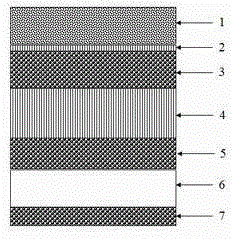
[0032] 1) ITO (Indium Tin Oxides) conductive glass is used as the light-transmitting / transparent electrode layer;
[0033] 2) The NiO layer was prepared on the surface of conductive glass by spraying pyrolysis technology. The thickness is controlled at 15nm;
[0034] 3) According to the molar ratio of 2:1:6, a mixed solution of nickel acetone hexanoate, lithium acetate, and magnesium acetate tetrahydrate was prepared, spin-coated on the transition layer, and dried at 350°C to prepare an electron transport layer; thickness 15nm;
[0035] 4) Prepare light-absorbing layer:
[0036] a. prepare PbI2 solution, concentration is 2.3Mol / L, and solvent is dimethylformamide;
[0037] b. Prepare CH3NH3I solution: the concentration is 7.5mg / mL, and the solvent is isopropanol;
[0038] In-situ synthesis of perovskite materials by solution method: spin-coat PbI2 solution on the electron transport layer first, dry it and soak it in CH3NH3I solution to grow perovskite materials, and obtain p...
Embodiment 2
[0048] 1) Aluminum zinc oxide AZO conductive glass is used as the light-transmitting / transparent electrode layer;
[0049] 2) Prepare a NiO2 layer on the surface of conductive glass by spraying thermal decomposition technology; the thickness is 8nm;
[0050] 3) A mixed solution of nickel hexanoate acetone, lithium acetate, and magnesium acetate tetrahydrate was prepared according to the molar ratio of 1:1:3, spin-coated on the transition layer, and dried at 400°C to prepare the electron transport layer; thickness 60nm;
[0051] 4) Prepare light absorbing layer:
[0052] a. Prepare PbI2 solution, the concentration is 0.5Mol / L, and the solvent is dimethylformamide;
[0053] b. Prepare CH3NH3I solution: the concentration is 10 mg / mL, and the solvent is isopropanol;
[0054] In-situ synthesis of perovskite materials by solution method: spin-coat PbI2 solution on the electron transport layer first, dry it and soak it in CH3NH3I solution to grow perovskite materials, and obtain p...
Embodiment 3
[0064] 1) Aluminum zinc oxide AZO conductive glass is used as the light-transmitting / transparent electrode layer;
[0065] 2) Prepare a NiO2 layer on the surface of conductive glass by spraying thermal decomposition technology; the thickness is 50nm;
[0066] 3) According to the molar ratio of 1:1:5, a mixed solution of nickel hexanoate acetone, lithium acetate, and magnesium acetate tetrahydrate was prepared, spin-coated on the transition layer, and dried at 300°C to prepare the electron transport layer; thickness Controlled at 10nm;
[0067] 4) Prepare light absorbing layer:
[0068] a. Prepare PbI2 solution, the concentration is 1.5Mol / L, and the solvent is dimethylformamide;
[0069] b. Prepare CH3NH3I solution: the concentration is 8.5 mg / mL, and the solvent is isopropanol;
[0070] In-situ synthesis of perovskite materials by solution method: spin-coat PbI2 solution on the electron transport layer first, dry it and soak it in CH3NH3I solution to grow perovskite materi...
PUM
 Abstract
Description
Claims
Application Information
 - R&D
- Intellectual Property
- Life Sciences
- Materials
- Tech Scout
- Unparalleled Data Quality
- Higher Quality Content
- 60% Fewer Hallucinations
Browse by: Latest US Patents, China's latest patents, Technical Efficacy Thesaurus, Application Domain, Technology Topic, Popular Technical Reports.
© 2025 PatSnap. All rights reserved.Legal|Privacy policy|Modern Slavery Act Transparency Statement|Sitemap|About US| Contact US: help@patsnap.com

