
Optical semiconductor integrated element and method for manufacturing same

An optical semiconductor and integrated component technology, which is applied to optical components, semiconductor lasers, semiconductor laser devices, etc., can solve the problems of increased optical transmission loss, peeling of mask 68, and reduced pattern accuracy, so as to reduce transmission loss and eliminate manufacturing. difficult effect

Inactive Publication Date: 2016-01-06
FUJITSU LTD
View PDF9 Cites 3 Cited by
  • Summary
  • Abstract
  • Description
  • Claims
  • Application Information

AI Technical Summary

Problems solved by technology

[0020] If such a protrusion occurs, the Figure 14 In the subsequent process, SiO is likely to be generated starting from the protruding part 2 Problems such as peeling off of the mask 68 and a decrease in pattern accuracy
In addition, in SiO 2 On the far side of the mask 66, the thickness of the i-type InP cladding layer 67 becomes thinner conversely, but in this case, there is a problem that the transmission loss of the light propagating through the waveguide becomes large.

Method used


Image

  • Optical semiconductor integrated element and method for manufacturing same
  • Optical semiconductor integrated element and method for manufacturing same
  • Optical semiconductor integrated element and method for manufacturing same

Examples


Embodiment 1

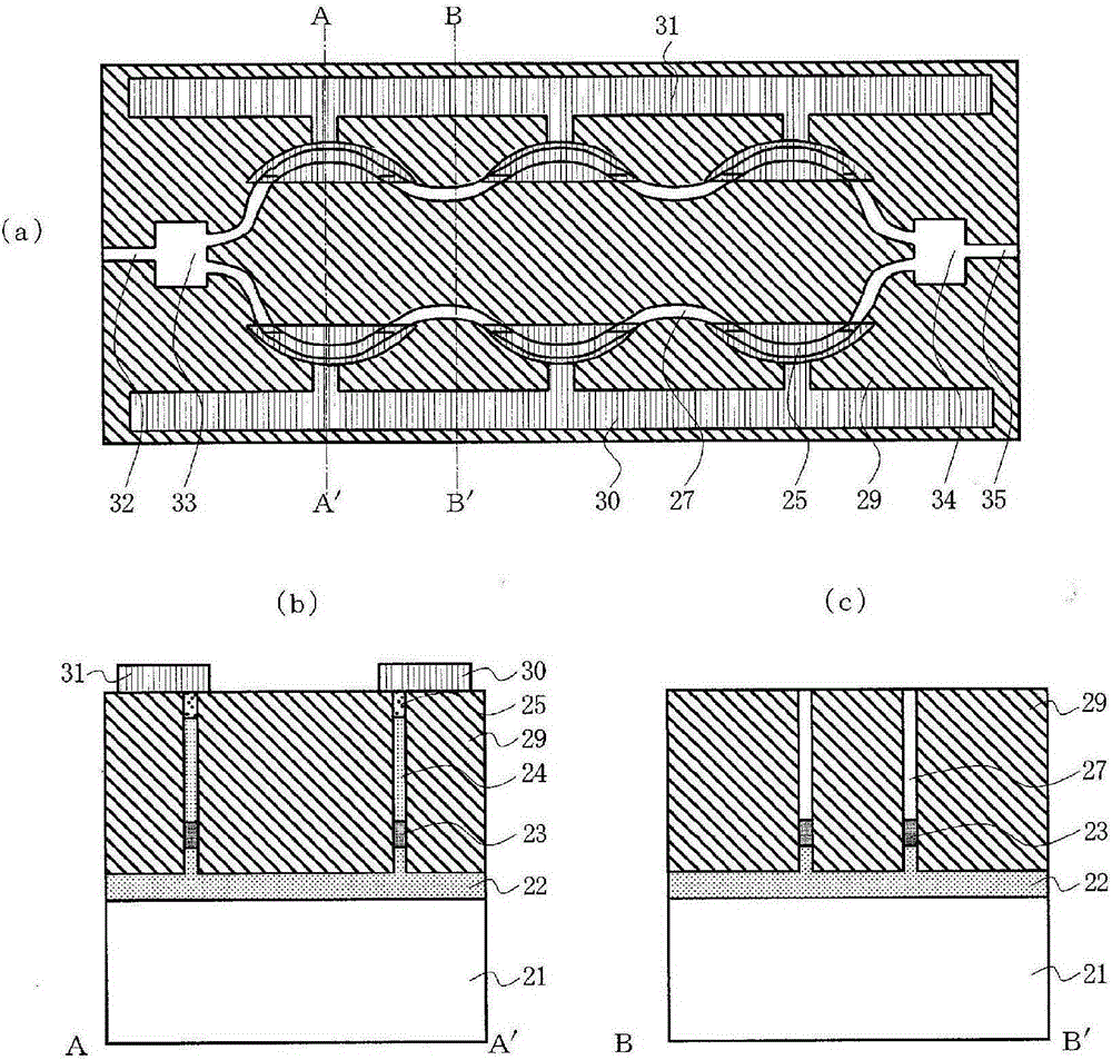
[0054]Next, refer to Figure 3 ~ Figure 6 , the capacity-loaded MZ modulator according to Embodiment 1 of the present invention will be described. image 3 is an explanatory diagram of a capacity loading type MZ modulator according to Embodiment 1 of the present invention, image 3 (a) is a top view, image 3 (b) for along image 3 A cross-sectional view of the dotted line connecting A-A' in (a), image 3 (c) for along image 3 Cross-sectional view of the dotted line connecting BB' in (a). This capacity-loaded MZ modulator includes an input waveguide 32 , a 1×2 MMI (multimode interference) waveguide 33 , two zigzag-shaped modulation waveguides, a 2×1 MMI waveguide 34 , and an output waveguide 35 .

[0055] The two modulation waveguides have a structure in which waveguide portions where electrodes 30 and 31 are formed and waveguide portions where no electrodes are formed are alternately arranged. Such as image 3 As shown in (b), the waveguide connected to the electrodes...

Embodiment 2

[0071] Next, refer to Figure 8 ~ Figure 11 , the optical semiconductor integrated element of Embodiment 2 of the present invention will be described, but here, it will be described as an optical semiconductor integrated element integrating a DFB (distributed feedback type) semiconductor laser and a semiconductor optical amplifier (SOA). Figure 8 It is an explanatory drawing of the optical semiconductor integrated element of Example 2 of the present invention, Figure 8 (a) is a top view, Figure 8 (b) for along Figure 8 A cross-sectional view of the dotted line connecting A-A' in (a), Figure 8 (c) for along Figure 8 Cross-sectional view of the dotted line connecting BB' in (a).

[0072] Such as Figure 8 As shown in (a), the waveguide constituting the DFB semiconductor laser and the waveguide constituting the semiconductor optical amplifier are arranged at the same position in a direction perpendicular to the direction in which the waveguides extend. In the separati...


PUM

PropertyMeasurementUnit
thicknessaaaaaaaaaa
thicknessaaaaaaaaaa
thicknessaaaaaaaaaa

Abstract

The present invention relates to an optical semiconductor integrated element and a method for manufacturing the optical semiconductor integrated element, solves difficulty in element manufacture, and reduces optical transmission loss. The present invention is provided with a stripe-shaped waveguide configured from a laminated structure wherein at least a first conductivity-type lower cladding layer, a waveguide core layer, and an upper cladding layer are laminated, and the upper cladding layer is formed using a second conductivity-type upper cladding layer, and an i-type upper cladding layer, which has a bent portion by being shifted in the perpendicular direction with respect to the main extending direction of the waveguide.

Description

technical field [0001] The present invention relates to an optical semiconductor integrated element and a manufacturing method thereof, and relates to an optical semiconductor integrated element that facilitates electrical separation between functional sections of an optical semiconductor integrated element in which a plurality of functional sections are monolithically integrated, for example, in one chip, and to manufacturing thereof method. Background technique [0002] In the current optical communication system, in order to cope with the increase of transmission capacity, for example, wavelength division multiplexing (WDM) communication using DP-QPSK (Dual Polarization Quadrature Phase Shift Keying: Dual Polarization Quadrature Phase Shift Keying) phase modulation signal is highly and complex. system. Along with this, there is a demand for higher functionality of optical semiconductor elements used in light sources for optical communication, and the like. [0003] As t...

Claims


Application Information

Patent Timeline
Patent Type & Authority Applications(China)
IPC IPC(8): G02F1/025G02B6/122G02B6/13G02F1/017H01S5/026H01S5/12
CPCG02F1/017G02F1/025G02B6/122H01S5/0265H01S5/101H01S5/12H01S5/2275H01S5/40H01S5/2213G02B6/131H01S5/026G02F1/212
Inventor 高林和雅山本刚之
Owner FUJITSU LTD
Learn More