


Quick Research
Generate reliable direction feasibility study reports for your R&D in just a few steps.

Technical Q&A
Discover and master advanced knowledge NOW. Basics, ideas, possibilities, all at once.

Find Solutions
As an expert in R&D theories, this can generate solutions to your technical problems instantly.

Evaluate Feasibility
Analyze your overall solution with one click, know your potential R&D risks in advance.

Monitor Landscape
Get weekly tech updates, stay abreast of the latest tech innovations and key insights.
Silica microlens and its manufacturing method
A technology of silicon dioxide and manufacturing methods, which is applied in the fields of lenses, optics, instruments, etc., can solve problems such as difficult to guarantee product consistency, unsuitable for mass production, lens surface shape distortion, etc., and achieve good product consistency and excellent Optical consistency, high transparency effect
- Summary
- Abstract
- Description
- Claims
- Application Information
AI Technical Summary
Problems solved by technology
Method used
Image

Examples
Embodiment 1
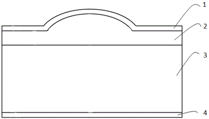
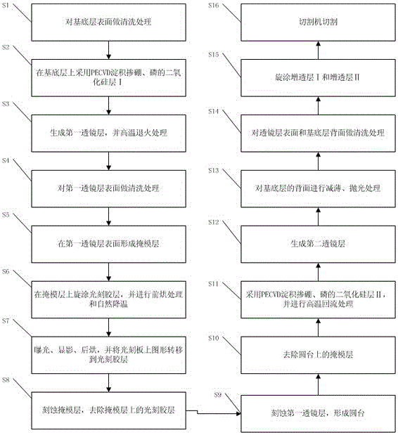
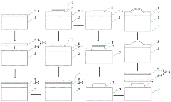
[0041] Embodiment 1: as figure 1 , image 3As shown, a silicon dioxide microlens includes a base layer 3 and a lens layer 2, the lens layer 2 is located on the front side of the base layer 3, and the base layer 3 and the lens layer 2 have the same refractive index. It also includes the anti-reflection layer I1 and the anti-reflection layer II4, the thickness of the anti-reflection layer I1 and the anti-reflection layer II4 are the same as 285nm, which is equal to a quarter of the wavelength of the light in the anti-reflection layer I1 or the anti-reflection layer II4 , so that the two reflected lights on the front and back surfaces of the anti-reflection layer I1 and the anti-reflection layer II4 cancel each other out.
[0042] The anti-reflection layer I1 covers the surface of the lens layer 2 , and the anti-reflection layer II4 covers the back of the base layer 3 . The cross-section of the lens layer 2 is plano-convex, including a first lens layer 2-2 and a second lens lay...
Embodiment 2
[0044] Embodiment 2: A silicon dioxide microlens, comprising a base layer and a lens layer, the lens layer is located on the front of the base layer, and also includes an anti-reflection layer I and an anti-reflection layer II, and the anti-reflection layer I covers the lens layer The anti-reflection layer II covers the back of the base layer; the lens layer includes a first lens layer and a second lens layer, and the second lens layer is wrapped on the first lens layer and fused together by high temperature reflow.
Embodiment 3
[0045] Embodiment 3: A silicon dioxide microlens, comprising a base layer and a lens layer, the lens layer is located on the front of the base layer, and also includes an anti-reflection layer I and an anti-reflection layer II, and the anti-reflection layer I covers the lens layer The anti-reflection layer II covers the back of the base layer; the lens layer includes a first lens layer and a second lens layer, and the second lens layer is wrapped on the first lens layer and fused together by high temperature reflow.
[0046] The material of the base layer is quartz glass material, which has good heat resistance, high transparency and excellent optical consistency; the material of the lens layer is silicon dioxide material doped with boron and phosphorus. It has good fluidity during high-temperature reflow; the material of the anti-reflection layer I and anti-reflection layer II is magnesium fluoride material, which has good anti-reflection effect and high coating uniformity.
PUM
 Abstract
Description
Claims
Application Information
 - R&D Engineer
- R&D Manager
- IP Professional
- Industry Leading Data Capabilities
- Powerful AI technology
- Patent DNA Extraction
Browse by: Latest US Patents, China's latest patents, Technical Efficacy Thesaurus, Application Domain, Technology Topic, Popular Technical Reports.
© 2024 PatSnap. All rights reserved.Legal|Privacy policy|Modern Slavery Act Transparency Statement|Sitemap|About US| Contact US: help@patsnap.com