Zero Voltage Switching Quasi-Resonant High Gain DC Boost Converter

A zero-voltage switching, DC boost technology, applied in the field of boost converters, can solve the problems of reduced circuit efficiency, increased voltage or current stress of switching devices, and increased switching loss of devices, and achieves simple circuit topology and switching loss. Reduction and switching noise reduction effect

Active Publication Date: 2018-01-26
SHANGHAI UNIVERSITY OF ELECTRIC POWER
View PDF3 Cites 0 Cited by
  • Summary
  • Abstract
  • Description
  • Claims
  • Application Information

AI Technical Summary

Problems solved by technology

However, with the increase of the switching frequency, because the switching loss is proportional to the switching frequency, the high frequency increases the switching loss of the device and reduces the circuit efficiency; The rate of change of current will generate severe electromagnetic interference (EMI); the voltage or current stress of switching devices will also increase, and the current and voltage overshoots generated by high-speed switching may cause the device's operating trajectory to exceed its safe operating area (SOA) and endanger Device Security
In view of the above reasons, it is difficult to meet the requirements of high efficiency, small size, low noise and low cost only by high frequency. It is necessary to improve the switching environment of the circuit where the device is located, so as to use the existing device to achieve low switching loss under high frequency conditions. soft switching

Method used


Image

  • Zero Voltage Switching Quasi-Resonant High Gain DC Boost Converter
  • Zero Voltage Switching Quasi-Resonant High Gain DC Boost Converter
  • Zero Voltage Switching Quasi-Resonant High Gain DC Boost Converter

Examples


Embodiment Construction

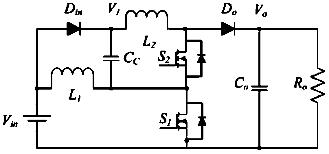
[0018] As shown in Figure 1, the topological example diagram of the high-gain DC boost converter under hard switching in the prior art, the converter input voltage V in The positive output is divided into two channels and respectively connected to the inductor L 1 One end and the diode D in Positive terminal, diode D in negative terminal and the inductor L 1 The other end is respectively connected to the charge pump capacitor C c across the charge pump capacitor C c Inductor L connected in series at both ends 2 and the main switch MOSFET S 2 , the charge pump capacitor C c with the main switching MOSFET S 2 connection point through the main switch MOSFET S 1 Connect to the converter input voltage V in Negative pole, inductance L 2 and the main switch MOSFET S 2 connection point through the freewheeling diode D o Connect to filter capacitor C o , filter capacitor C o Parallel load R at both ends o .

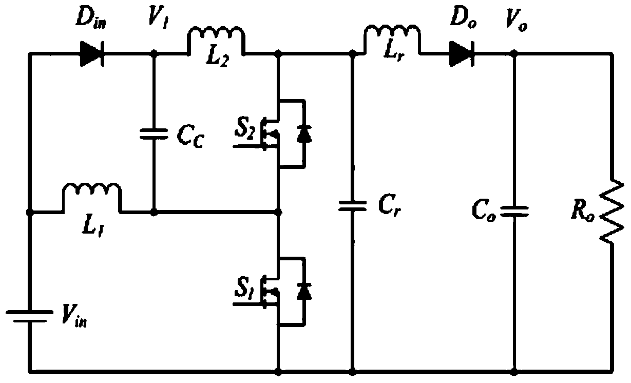
[0019] Such as figure 2 The topology example diagram of the...


PUM


Abstract

The invention relates to a zero-voltage switching quasi-resonance high-gain DC boost converter. An LC resonance circuit is added at the rear ends of main switches S1 and S2 and the front end of an output load of an improved boost DC converter under a hard switching condition, thus, a soft switching condition is formed, the switching environment of circuits in which devices are positioned is improved, and voltage and current change rates during the switching process are slowed via resonance; voltages at both ends of each of the main switches S1 and S2 are reduced to zero before the main switches S1 and S2 are switched on, so that the switching loss and switching noise are reduced; circuit efficiency under the soft switching condition is high when comparing input / output power under the hard switching condition in the prior art and under the soft switching condition provided by the invention; the circuit topological structure is simple; and the zero-voltage switching quasi-resonance high-gain DC boost converter can satisfy requirements of being simple and efficient, light in weight and low in noise when compared with the improved boost DC converter under the hard switching condition in the prior art.

Description

technical field [0001] The invention relates to a boost converter, in particular to a zero-voltage switch quasi-resonant high-gain DC boost converter. Background technique [0002] With the development of power electronics technology, higher requirements are put forward for the volume, efficiency and electromagnetic compatibility of power electronic devices. The main components of power electronic devices, such as filter inductors, capacitors and transformers, are inversely proportional to the square root of the power supply frequency. Therefore, under the trend of power electronic devices developing towards modularization and miniaturization, it is necessary to increase the switching frequency. However, with the increase of the switching frequency, because the switching loss is proportional to the switching frequency, the high frequency increases the switching loss of the device and reduces the circuit efficiency; The rate of change of current will generate severe electrom...

Claims


Application Information

Patent Timeline
Patent Type & Authority Patents(China)
IPC IPC(8): H02M3/07
Inventor 屈克庆冯苗苗潘雪涛赵晋斌梁晓霞
Owner SHANGHAI UNIVERSITY OF ELECTRIC POWER
Why Eureka
Try Eureka