Junction field effect transistor and method of making same

A technology of field effect transistors and junctions, applied in the preparation of junction field effect transistors, in the field of junction field effect transistors, can solve the problem of high pinch-off voltage

Active Publication Date: 2017-12-12
CSMC TECH FAB2 CO LTD
View PDF6 Cites 0 Cited by
  • Summary
  • Abstract
  • Description
  • Claims
  • Application Information

AI Technical Summary

Problems solved by technology

Conventional JFETs have a high pinch-off voltage

Method used


Image

  • Junction field effect transistor and method of making same
  • Junction field effect transistor and method of making same
  • Junction field effect transistor and method of making same

Examples


Embodiment Construction

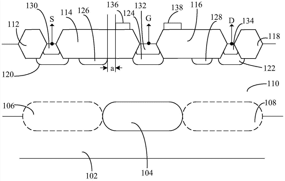
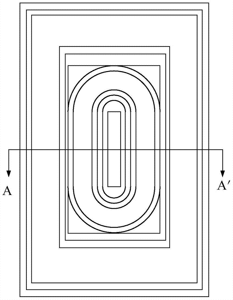
[0019] In order to make the objects, features and advantages of the present invention more comprehensible, specific implementations of the present invention will be described in detail below in conjunction with the accompanying drawings. In this specification and drawings, reference signs N and P assigned to layers or regions indicate that these layers or regions include a large number of electrons or holes, respectively. Further, the reference marks + and − assigned to N or P indicate that the concentration of the dopant is higher or lower than in layers not so assigned to the marks. In the following description of the preferred embodiments and the drawings, similar components are assigned similar reference numerals and redundant descriptions thereof are omitted here.

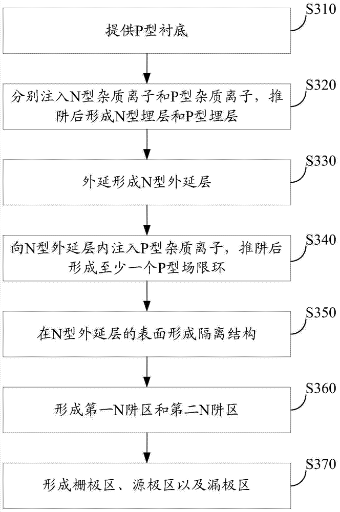
[0020] A junction field effect transistor, comprising: a P-type substrate; a P-type buried layer and an N-type buried layer placed on the P-type substrate. Wherein, the N-type buried layer is respectively pla...


PUM


Abstract

The invention discloses a junction field effect transistor, comprising: a P-type substrate; a P-type buried layer and an N-type buried layer; the N-type buried layer is placed on both sides of the P-type buried layer; an N-type epitaxial layer; The first isolation structure, the second isolation structure, the third isolation structure and the fourth isolation structure on the N-type epitaxial layer; the source region placed between the first isolation structure and the second isolation structure; placed in the source region The first N well region below; the gate region placed between the second isolation structure and the third isolation structure; the drain region placed between the third isolation structure and the fourth isolation structure; placed under the drain region The second N-well region; also includes at least one P-type field confinement ring placed on the N-type epitaxial layer and located between the source region and the drain region. The above junction field effect transistor can realize the effect of Triple RESURF, can effectively reduce the pinch-off voltage, and realize the purpose of low pinch-off voltage. The invention also discloses a preparation method of the junction field effect transistor.

Description

technical field [0001] The invention relates to the technical field of semiconductors, in particular to a junction field effect transistor and a preparation method of the junction field effect transistor. Background technique [0002] BCD is a monolithic integration process technology, which can prepare bipolar transistor (Bipolar Junction Transistor) CMOS and DMOS devices on the same chip. In the BCD process, the Junction Field Effect Transistor (JFET) is a very important type of device. Using the Junction Field Effect Transistor can easily build a start-up module and a constant current source module. For JFETs, the pinch-off voltage is one of the key parameters. Conventional JFETs have a high pinch-off voltage. Contents of the invention [0003] Based on this, it is necessary to provide a junction field effect transistor with low pinch-off voltage to solve the above problems. [0004] Also provided is a preparation method of the junction field effect transistor. [0...

Claims


Application Information

Patent Timeline
Patent Type & Authority Patents(China)
IPC IPC(8): H01L29/808H01L21/337
Inventor 祁树坤张广胜
Owner CSMC TECH FAB2 CO LTD
Why Eureka
Try Eureka