Filter and manufacturing method thereof

A technology of filters and metal layers, which is applied in waveguide devices, resonators, circuits, etc., can solve the problems of large size of planar PCB circuits and cannot meet the requirements of wireless communication, and achieve the effect of compact structure and easy implementation

Active Publication Date: 2015-11-25
INST OF MICROELECTRONICS CHINESE ACAD OF SCI
View PDF5 Cites 4 Cited by
  • Summary
  • Abstract
  • Description
  • Claims
  • Application Information

AI Technical Summary

Problems solved by technology

[0004] Distributed transmission lines were first used in planar PCB circuit boards, mainly including microstrip line structure, coplanar waveguide (CPW) structure, slot line and defect ground (DGS) structure, which are widely used and mature, but the size of planar PCB circuit is too large. Large, unable to meet the requirements of modern wireless communication technology

Method used


Image

  • Filter and manufacturing method thereof
  • Filter and manufacturing method thereof
  • Filter and manufacturing method thereof

Examples


Embodiment 1

[0038] In this embodiment, the resonant cavity is a U-shaped slot line formed in the metal layer, and the input and output feed lines of the coplanar waveguide are formed in the same metal layer. The structure is compact, easy to integrate in the integrated circuit process, and can Perform strong coupling power supply to achieve wide bandwidth and low insertion loss performance.

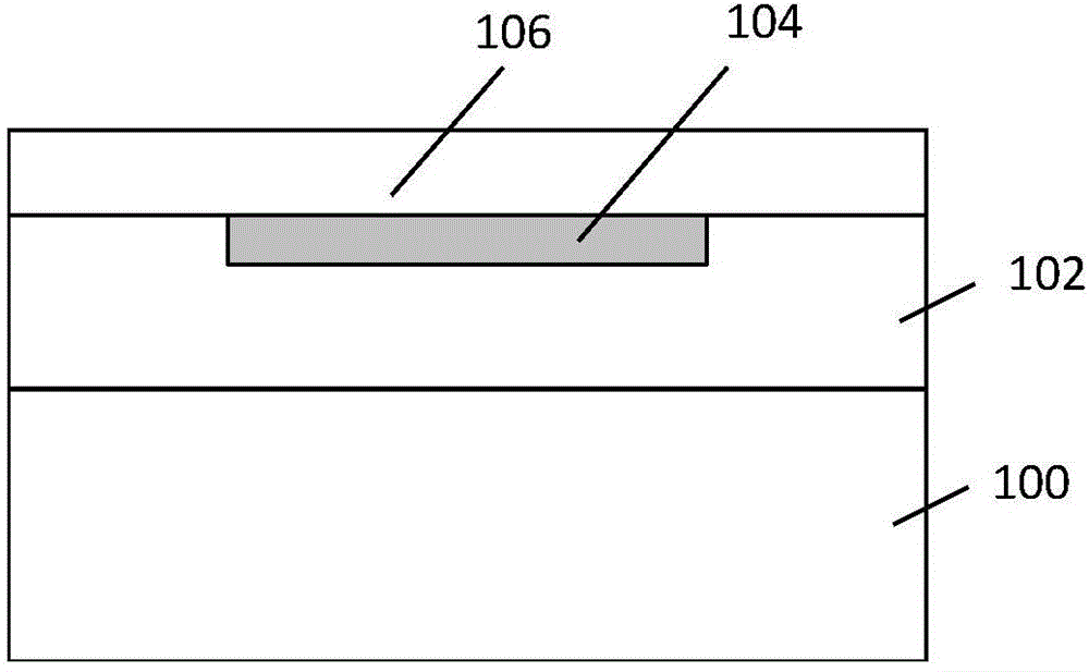
[0039] In this example, refer to figure 1 As shown, the filter includes:

[0040] substrate 100;

[0041] a dielectric layer 102 on the substrate;

[0042] the first metal layer 104 in the dielectric layer; and

[0043] A slot line resonator and input and output feed lines are formed in the first metal layer 104 .

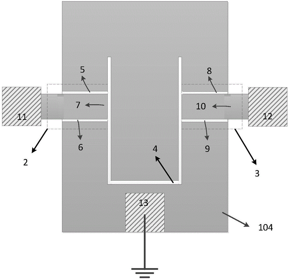
[0044] Such as figure 2 As shown, it is a top view of the first metal layer, and the resonant cavity 4 , the input feeder 2 and the output feeder 3 are formed in the first metal layer 104 .

[0045] In this embodiment, the resonant cavity is a slot line resonator 4 formed in the fi...

Embodiment 2

[0064] In this embodiment, the resonant cavity is a U-shaped slot line formed in a metal layer, and the input and output feed lines of the microstrip line are formed in another metal layer.

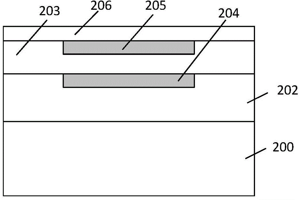
[0065] In this example, refer to image 3 As shown, the filter includes:

[0066] substrate 200;

[0067] The first dielectric layer 202 on the substrate, and the first metal layer 204 in the first dielectric layer 202;

[0068] A second dielectric layer 203 on the first dielectric layer 202, a second metal layer 205 in the second dielectric layer on the first metal layer;

[0069] Wherein, the slot line resonant cavity is formed in the first metal layer 204, and the second metal layer 205 is the input feed line and the output feed line of the microstrip transmission line.

[0070] Such as Figure 4 As shown, it is a top view of the first metal layer, which is the same as the resonant cavity structure in Embodiment 1. A slot line resonator 4 is formed in the first metal layer 104, whi...


PUM


Abstract

The present invention provides a filter comprising a substrate, a dielectric layer on the substrate, a first metal layer in the dielectric layer, a trough-line resonant cavity formed in the first metal layer to expose the dielectric layer under the first metal layer, an input feed line and an output feed line. According to the technical scheme of the invention, the trough-line resonant cavity is formed in the metal layer, so that signals can be transmitted via trough-lines. Therefore, the signal filtering effect is realized. The filter is compact in structure and can be easily manufactured through the integrated circuit process.

Description

technical field [0001] The invention relates to the field of semiconductor devices and filters, in particular to a filter. Background technique [0002] In the field of wireless communication, the filter is a key passive device. The bandpass characteristic of the filter can separate the spectrum resource space, and the bandstop characteristic can eliminate the electromagnetic interference outside the working frequency band. [0003] With the improvement of the integration of radio frequency circuits and the continuous progress of material science and manufacturing technology, the size of wireless communication circuits is becoming smaller and smaller, gradually developing towards chip, integration, and modularization. Higher requirements are also put forward for the key passive component filters in wireless communication circuits. [0004] Distributed transmission lines were first used in planar PCB circuit boards, mainly including microstrip line structure, coplanar wavegu...

Claims


Application Information

Patent Timeline
Patent Type & Authority Applications(China)
IPC IPC(8): H01P1/207H01P11/00H01P7/06
Inventor 万晶牟鹏飞阎跃鹏
Owner INST OF MICROELECTRONICS CHINESE ACAD OF SCI
Why Eureka
Try Eureka