Display panel and manufacturing method thereof

A manufacturing method and technology for display panels, which are applied in the manufacture of semiconductor/solid-state devices, electrical components, and electrical solid-state devices, etc., can solve the problems of small grain size and low carrier mobility, reduce grain boundaries, improve performance, The effect of improving carrier mobility

Active Publication Date: 2015-11-25
TCL CHINA STAR OPTOELECTRONICS TECH CO LTD
View PDF9 Cites 5 Cited by
  • Summary
  • Abstract
  • Description
  • Claims
  • Application Information

AI Technical Summary

Problems solved by technology

[0004] The invention mainly solves the problem that the crystal grains in the polysilicon film of the display panel in the prior art are small and the carrier mobility is small caused by many grain boundaries

Method used


Image

  • Display panel and manufacturing method thereof
  • Display panel and manufacturing method thereof
  • Display panel and manufacturing method thereof

Examples


Embodiment Construction

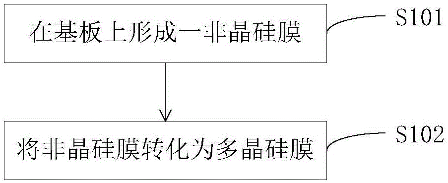
[0024] refer to figure 1 , figure 1 is a schematic flow chart of the first embodiment of the manufacturing method of the display panel of the present invention, the manufacturing method in this embodiment mainly includes the following steps:

[0025] S101: forming an amorphous silicon film on a substrate.

[0026] The substrate can be a quartz substrate or a glass substrate. The quartz substrate can withstand a higher temperature than the glass substrate. In the traditional process, when transforming amorphous silicon into polysilicon, a temperature above 600°C is required. At this temperature, the glass substrate It is easy to soften and deform, so quartz substrates are generally used. However, the price of quartz substrates is much higher than that of glass substrates. When the size of display panels becomes larger and larger, that is, the required substrates are also larger and larger. Based on cost considerations, glass substrates must be used. At this time, low-temperat...


PUM


Abstract

The invention discloses a display panel and a manufacturing method thereof. The manufacturing method of the display panel comprises the following steps: forming a non-crystalline silicon film on a substrate, wherein the non-crystalline silicon film comprises at least two non-crystalline silicon layers, and the crystalline grain densities of the two adjacent non-crystalline silicon layers are different; and converting the non-crystalline silicon film into a polycrystalline film. The polycrystalline film with lager crystalline grains and fewer grain boundaries is obtained in the manufacturing method, so that the carrier mobility of the polycrystalline film is higher, and the performance of the corresponding display panel is better.

Description

technical field [0001] The present invention relates to the field of display technology, in particular to a display panel and a manufacturing method thereof. Background technique [0002] At present, liquid crystal display technology is developing rapidly, and the application of thin film transistors makes liquid crystal display become the mainstream of flat-panel display, which is applied to personal computers, monitors, game consoles and other products. Amorphous silicon thin film transistors are widely used because they can be produced at a low temperature of 200°C-300°C. However, the low carrier mobility of amorphous silicon makes amorphous silicon thin film transistors unable to meet the needs of current high-speed component applications. Therefore, At present, polysilicon thin film transistors are mostly used, and their relatively high carrier mobility and low temperature sensitivity make them more suitable for high-speed components. [0003] The current way to obtain...

Claims


Application Information

Patent Timeline
Patent Type & Authority Applications(China)
IPC IPC(8): H01L21/77H01L27/12
CPCH01L27/1229H01L27/1274H01L27/1281H01L21/02422H01L21/0245H01L21/02488H01L21/02502H01L21/02532H01L21/02675H01L21/02592H01L21/0262H01L29/04
Inventor 张旭东
Owner TCL CHINA STAR OPTOELECTRONICS TECH CO LTD
Why Eureka
Try Eureka