
Design method for increasing PCB yield

A design method and yield rate technology, applied in the electronic field, to achieve the effect of controlling R&D costs and improving yield rate

Inactive Publication Date: 2015-11-25
SUZHOU R&D CENT OF NO 214 RES INST OF CHINA NORTH IND GRP
View PDF2 Cites 1 Cited by
  • Summary
  • Abstract
  • Description
  • Claims
  • Application Information

AI Technical Summary

Problems solved by technology

[0004] In order to solve the technical problems existing in the prior art, the present invention provides a PCB design method to improve the bad situation in the process of processing

Method used


Image

  • Design method for increasing PCB yield
  • Design method for increasing PCB yield
  • Design method for increasing PCB yield

Examples


Embodiment Construction

[0016] The present invention will be further described below in conjunction with the accompanying drawings. The following examples are only used to illustrate the technical solution of the present invention more clearly, but not to limit the protection scope of the present invention.

[0017] An embodiment proposed by the present invention effectively improves the yield of PCB by changing the distance between device pins and copper cladding on the printed circuit board, thereby effectively controlling the research and development cost of the entire project.

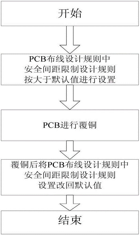
[0018] The concrete design process of PCB of the present invention is as figure 2 , the design steps are as follows:

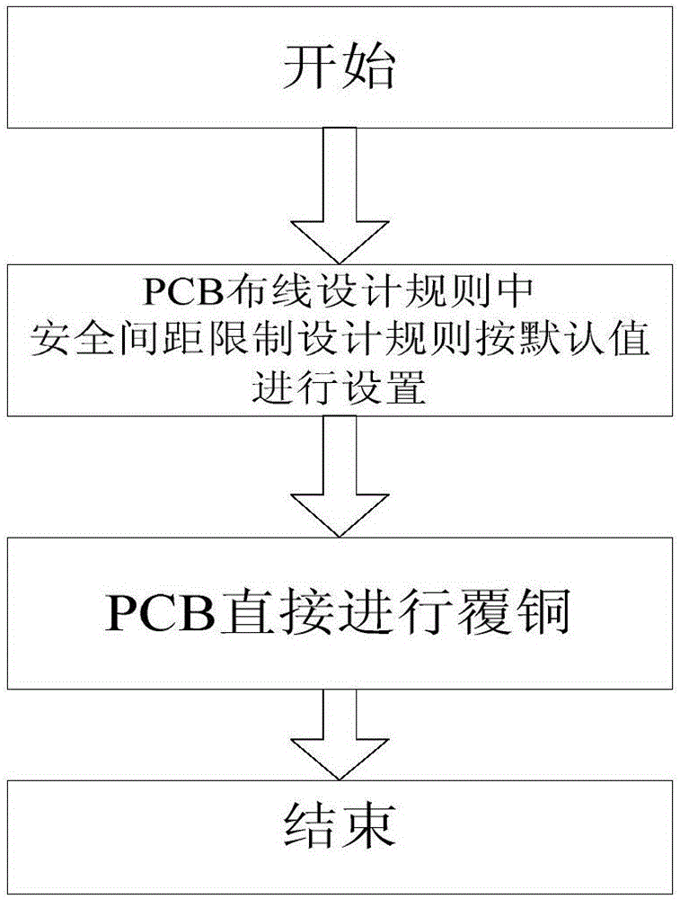
[0019] 1) Carry out PCB wiring according to the PCB wiring process;

[0020] 2) Set the safety spacing adjustment in the PCB layout design rules to be greater than the default value;

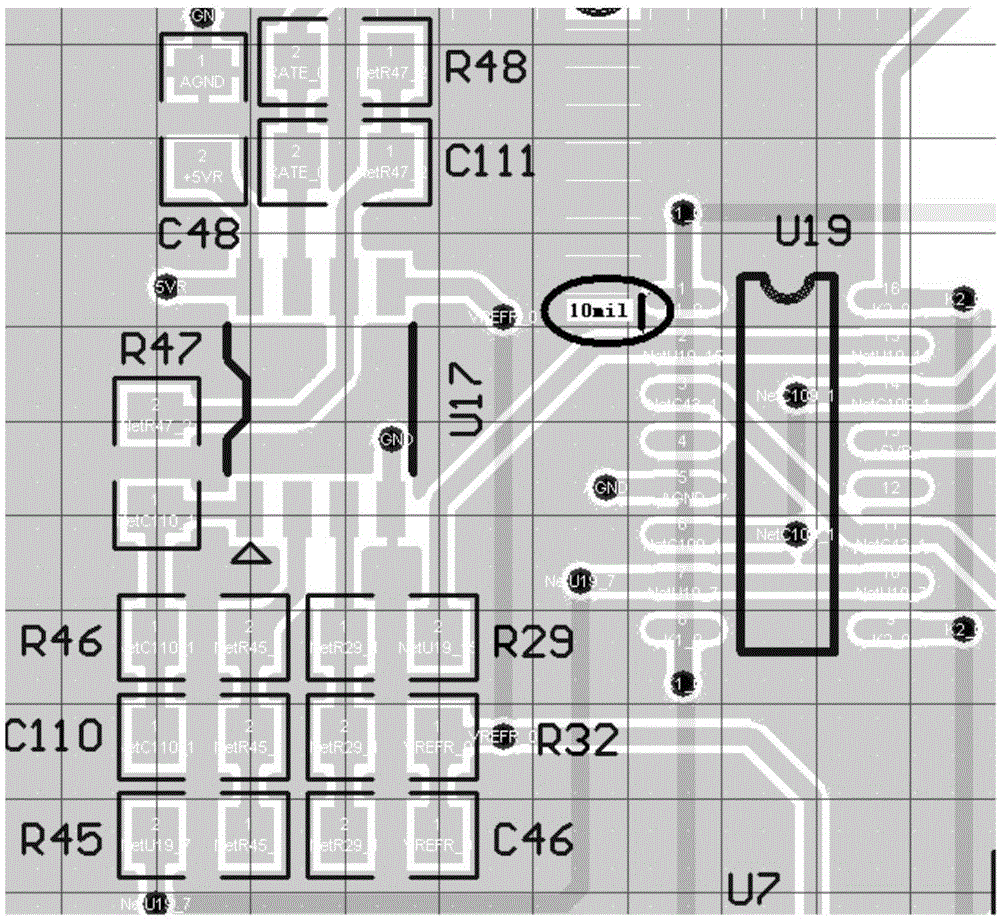
[0021] 3) The PCB is covered with copper, so that when the copper is poured, the new rules between the pin and the li...


PUM


Abstract

The invention discloses a design method for increasing the PCB yield. The method comprises the following steps: 1) performing PCB wiring according to a PCB wiring process; 2) setting safety spacing in a PCB wiring design rule to be greater than a default value; 3) performing copper coating on the PCB; and 4) modifying the safety spacing in the PCB wiring design rule to be the default value by limiting the design rule after the PCB is subjected to copper coating. According to the design method for increasing the PCB yield, the distance between a device pin on the PCB and coating copper is changed to effectively increase the PCB yield so as to effectively control the research and development costs of the whole project.

Description

technical field [0001] The invention relates to a design method for improving PCB yield, which belongs to the field of electronic technology. Background technique [0002] In the current printed circuit board (referred to as PCB) design, devices with small pin spacing and copper clad may be used, but such devices are designed according to conventional PCBs, such as figure 1 . In the process of processing, there will be misconnection of pins and copper cladding, which will increase the defective rate of PCB processing. If the distance between the device pin and the copper pour is very close, according to the conventional PCB design, the connection between the pin and the copper pour will occur during the processing process, which will lead to an increase in the defective rate of PCB processing. [0003] By improving the processing technology, the defect rate of PCB processing can be effectively reduced, but at the same time, the design cost will be greatly increased, result...

Claims


Application Information

Patent Timeline
IPC IPC(8): G06F17/50
Inventor 王丽唐兴刚童紫平
Owner SUZHOU R&D CENT OF NO 214 RES INST OF CHINA NORTH IND GRP
Learn More