


Quick Research
Generate reliable direction feasibility study reports for your R&D in just a few steps.

Technical Q&A
Discover and master advanced knowledge NOW. Basics, ideas, possibilities, all at once.

Find Solutions
As an expert in R&D theories, this can generate solutions to your technical problems instantly.

Evaluate Feasibility
Analyze your overall solution with one click, know your potential R&D risks in advance.

Monitor Landscape
Get weekly tech updates, stay abreast of the latest tech innovations and key insights.
Release film for manufacturing printed circuit board and method for producing release film for manufacture of printed circuit board
A technology for printed circuit substrates and peeling films, applied in the directions of manufacturing tools, chemical instruments and methods, applications, etc., can solve problems such as difficulty in obtaining reliable printed circuit substrates, and achieve failure prevention, high manufacturing reliability, and pinhole prevention. or the effect of local uneven thickness
- Summary
- Abstract
- Description
- Claims
- Application Information
AI Technical Summary
Problems solved by technology
Method used
Image

Examples
Embodiment 1
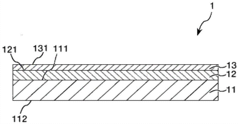
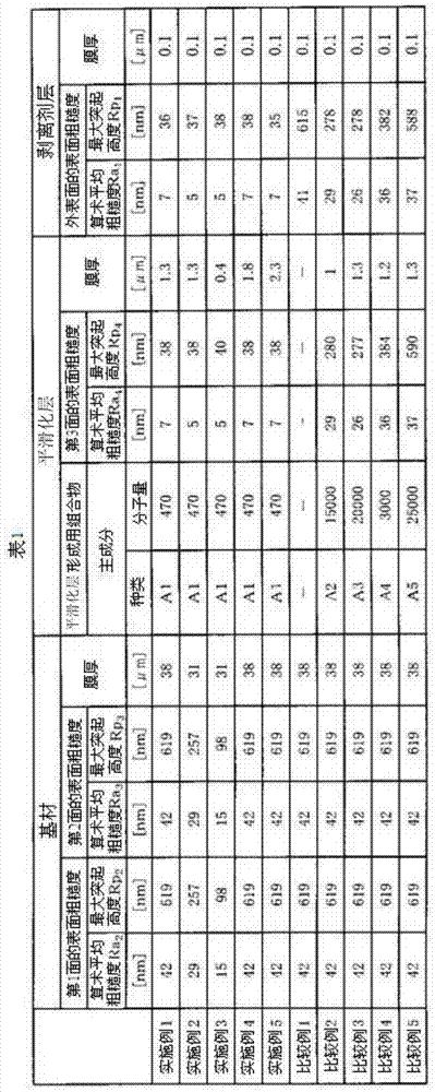
[0150] First, prepare a biaxially stretched polyethylene terephthalate film [thickness: 38 μm, arithmetic average roughness Ra of the first surface] as a base material 2 : 42nm, the maximum protrusion height Rp of the first surface 2 : 619nm, the arithmetic mean roughness Ra of the second surface 3 : 42nm, the maximum protrusion height Rp of the second surface 3 : 619nm].
[0151] Then, an ultraviolet-curable compound [manufactured by Arakawa Chemical Industry Co., Ltd., trade name "Bi-Mset 575CB"] mainly composed of urethane acrylate oligomer as an active energy ray-curable compound, 100% by mass of solid content, Mass average molecular weight 470, containing photoinitiator] 100 mass parts, and toluene, methyl ethyl ketone were mixed, and the composition for smoothing layer formation of 20 mass % of solid content was obtained.
[0152] The obtained composition for smoothing layer formation was apply|coated on the 1st surface of a base material with the No. 4 Meyer bar, and...
Embodiment 2
[0156] Except that the biaxially stretched polyethylene terephthalate film of Example 1 was converted into a biaxially stretched polyethylene terephthalate film [thickness: 31 μm, arithmetic mean roughness of the first surface Degree Ra 2 : 29nm, the maximum protrusion height Rp of the first surface 2 : 257nm, the arithmetic mean roughness Ra of the second surface 3 : 29nm, the maximum protrusion height Rp of the second surface 3 : 257 nm], a release film for printed circuit board manufacture was obtained in the same manner as in Example 1.
Embodiment 3
[0158] Except that the biaxially stretched polyethylene terephthalate film of Example 1 was converted into a biaxially stretched polyethylene terephthalate film [thickness: 31 μm, arithmetic mean roughness of the first surface Degree Ra 2 : 15nm, the maximum protrusion height Rp of the first surface 2 : 98nm, the arithmetic mean roughness Ra of the second surface 3 : 15nm, the maximum protrusion height Rp of the second surface 3 : 98 nm], except that the thickness of the smoothing layer was changed to 0.4 μm, a release film for printed circuit board production was obtained in the same manner as in Example 1.
PUM
| Property | Measurement | Unit |
|---|---|---|
| thickness | aaaaa | aaaaa |
| surface roughness | aaaaa | aaaaa |
| surface roughness | aaaaa | aaaaa |
Abstract
Description
Claims
Application Information
 - R&D Engineer
- R&D Manager
- IP Professional
- Industry Leading Data Capabilities
- Powerful AI technology
- Patent DNA Extraction
Browse by: Latest US Patents, China's latest patents, Technical Efficacy Thesaurus, Application Domain, Technology Topic, Popular Technical Reports.
© 2024 PatSnap. All rights reserved.Legal|Privacy policy|Modern Slavery Act Transparency Statement|Sitemap|About US| Contact US: help@patsnap.com